Home > Press > Study Produces Road Map for Nanomanufacturing
Abstract:
Systematic study of cadmium selenide nanostructure growth guides future efforts
Study Produces Road Map for Nanomanufacturing
Atlanta, GA | October 31, 2005
Researchers have taken an important step toward high-volume production of new nanometer-scale structures with the first systematic study of growth conditions that affect production of one-dimensional nanostructures from the optoelectronic material cadmium selenide (CdSe).
Using the results from more than 150 different experiments in which temperature and pressure conditions were systematically varied, nanotechnology researchers at the Georgia Institute of Technology created a �road map� to guide future nanomanufacturing using the vapor-liquid-solid (VLS) technique.
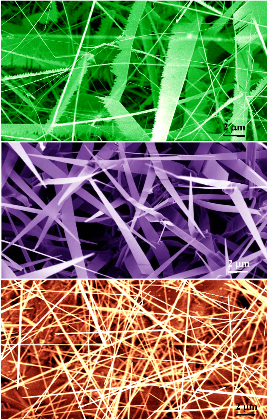
Scanning electron microscope images show nanosaws, nanobelts and nanowires of cadmium selenide grown using the vapor-liquid-solid process. Copyright © Georgia Institute of Technology
|
The results, reported this month in the journal Advanced Materials (Vol. 17, pp.1-6), join earlier Georgia Tech work that similarly mapped production conditions for nanostructures made from zinc oxide � an increasingly important nanotechnology material. Together, the two studies provide a foundation for large-scale, controlled synthesis of nanostructures that could play important roles in future sensors, displays and other nanoelectronic devices.
The research was supported by the National Science Foundation (NSF), the NASA Vehicle Systems Program, the Department of Defense Research and Engineering (DDR&E) and the Defense Advanced Research Projects Agency (DARPA).
�For the future of nanomanufacturing, we needed a systematic map to show the best conditions for producing these structures reproducibly with high yield,� explained Zhong Lin Wang, director of Georgia Tech�s Center for Nanoscience and Nanotechnology. �This information will be necessary for scaling up the production of these interesting structures for the applications that will be developed.�
In work that required more than a year to complete, Wang and collaborator Christopher Ma collected information on more than 45 separate combinations of growth conditions governing the production of cadmium selenide nanostructures. In their experimental set-up, powdered cadmium selenide was heated to hundred of degrees Celsius in a simple horizontal tube furnace under the flow of nitrogen gas, using gold as a catalyst.
The technique produced three different types of nanostructures:
- �Nanosaws/nanocombs,� unusual structures that form with �teeth� on one side and a smooth surface on the other
- �Nanobelts,� which are ribbon-like structures
- �Nanowires� that resemble grass and grow vertically from the substrate.
The researchers varied the temperature at the cadmium selenide source, the temperature of the silicon substrate where the structures grew, and the gas pressure inside the furnace. They repeated each experimental condition three times, each time determining where the structures grew on the substrate and counting the number of nanosaws/nanocombs, nanobelts and nanowires in samples that were examined with electron microscopy.
�These three different structures are all produced using the same general experimental conditions, but somehow you get different percentages of each,� Wang said. �Our goal was to determine how to control the conditions to learn how to get close to 100 percent yield of each structure. This required a systematic study of the experimental conditions.�
Each experiment required approximately two days to produce the structures and analyze the samples.
Based on their experimental work, Wang and Ma mapped the optimal conditions for producing each of the three structures � and learned more about the fabrication process. For instance, they found that growth of the nanostructures is primarily controlled by the nitrogen gas pressure inside the chamber and the temperature of the substrate where the structures are deposited. They also learned where each type of structure was likely to be deposited on the substrate under each set of conditions.
Cadmium selenide nanosaws and nanocombs are the most finicky to grow. At the other end of the scale, nanowires can be produced from cadmium selenide at a broad range of temperature and pressure conditions. Specifically, the researchers reported:
- Lower temperatures at the source material (630 degrees C), higher pressures (600 millibars) and substrate temperatures of approximately 575 degrees C produce the highest percentage of nanosaws and nanocombs.
- Lower temperatures at the source material (700 degrees C), lower chamber pressures (4 millibars) and substrate temperatures of approximately 575 degrees C produce the highest percentage of nanobelts.
- Growth of nanowires can be carried out at a broad range of temperatures and pressures, with higher source temperatures favoring the growth of nanowires over nanosaws.
If other groups want to produce these structures, they can use our plots to determine the pressures that will be required, the temperatures and the locations within the chamber where they will grow,� Wang said. �Until now, researchers have had to determine these parameters by trial and error.�
Cadmium selenide has been studied for applications in optoelectronics, luminescent materials, lasing materials and biomedical imaging. It is perhaps best known as the basis for quantum dots that have applications in biomedical imaging.
Zinc oxide is a semiconducting, piezoelectric and optical material with potential applications in sensors, resonators and other nanoelectronic structures. The systematic study of growth parameters for these structures involved more than 100 experiments and was published in the Journal of Physical Chemistry (B, Vol. 109 (2005) 9869-9872).
�Now that we have determined the optimal requirements for growth, it should be straightforward to scale up the production of these structures,� Wang concluded. �We have a lot of ideas for potential applications.�
Technical Contact:
Zhong Lin Wang
404-894-8008
zhong.wang@mse.gatech.edu
Research News & Publications Office
Georgia Institute of Technology
75 Fifth Street, N.W., Suite 100
Atlanta, Georgia 30308 USA
Related Links:
Zhong Lin Wang
Center for Nanoscience and Nanotechnology
School of Materials Science and Engineering
About Georgia Institute of Technology:
The Georgia Institute of Technology is one of the nation's premiere research universities. Ranked ninth among U.S. News & World Report's top public universities, Georgia Tech educates more than 17,000 students every year through its Colleges of Architecture, Computing, Engineering, Liberal Arts, Management and Sciences. Tech maintains a diverse campus and is among the nation's top producers of women and African-American engineers. The Institute offers research opportunities to both undergraduate and graduate students and is home to more than 100 interdisciplinary units plus the Georgia Tech Research Institute. During the 2004-2005 academic year, Georgia Tech reached $357 million in new research award funding.
For more information, please click here
John Toon
404-894-6986
john.toon@edi.gatech.edu
Jane Sanders
404-894-2214
jane.sanders@edi.gatech.edu
Copyright � Georgia Institute of Technology
If you have a comment, please Contact us.
Issuers of news releases, not 7th Wave, Inc. or Nanotechnology Now, are solely responsible for the accuracy of the content.
Bookmark:


| Related News Press |
Preparing for Nano
![]() Disruptive by Design: Nano Now February 1st, 2019
Disruptive by Design: Nano Now February 1st, 2019
![]() How nanoscience will improve our health and lives in the coming years: Targeted medicine deliveries and increased energy efficiency are just two of many ways October 26th, 2016
How nanoscience will improve our health and lives in the coming years: Targeted medicine deliveries and increased energy efficiency are just two of many ways October 26th, 2016
![]() Searching for a nanotech self-organizing principle May 1st, 2016
Searching for a nanotech self-organizing principle May 1st, 2016
Materials/Metamaterials/Magnetoresistance
![]() First real-time observation of two-dimensional melting process: Researchers at Mainz University unveil new insights into magnetic vortex structures August 8th, 2025
First real-time observation of two-dimensional melting process: Researchers at Mainz University unveil new insights into magnetic vortex structures August 8th, 2025
![]() Researchers unveil a groundbreaking clay-based solution to capture carbon dioxide and combat climate change June 6th, 2025
Researchers unveil a groundbreaking clay-based solution to capture carbon dioxide and combat climate change June 6th, 2025
![]() A 1960s idea inspires NBI researchers to study hitherto inaccessible quantum states June 6th, 2025
A 1960s idea inspires NBI researchers to study hitherto inaccessible quantum states June 6th, 2025
![]() Institute for Nanoscience hosts annual proposal planning meeting May 16th, 2025
Institute for Nanoscience hosts annual proposal planning meeting May 16th, 2025
Announcements
![]() Decoding hydrogen‑bond network of electrolyte for cryogenic durable aqueous zinc‑ion batteries January 30th, 2026
Decoding hydrogen‑bond network of electrolyte for cryogenic durable aqueous zinc‑ion batteries January 30th, 2026
![]() COF scaffold membrane with gate‑lane nanostructure for efficient Li+/Mg2+ separation January 30th, 2026
COF scaffold membrane with gate‑lane nanostructure for efficient Li+/Mg2+ separation January 30th, 2026
|
|
||
|
|
||
| The latest news from around the world, FREE | ||
|
|
||
|
|
||
| Premium Products | ||
|
|
||
|
Only the news you want to read!
Learn More |
||
|
|
||
|
Full-service, expert consulting
Learn More |
||
|
|
||