Home > Nanotechnology Columns > NanoNewsNet.ru > Next step in nanotechnology instrumentation: Atomic Force Microscopy and X-Ray Fluorescence Analysis Integration
 |
Eugene Birger Principal Analyst NanoNewsNet.ru |
Abstract:
During last 20-30 years the instruments that explore or probe the surface of ultra-small samples have steadily proliferated. Physicists, chemists, and molecular biologists working in nanoscience have had to familiarize themselves with microscopes that use thermal, magnetic, capacitive, and electrochemical properties. What is next for this amazing family of SPM?
July 10th, 2010
Next step in nanotechnology instrumentation: Atomic Force Microscopy and X-Ray Fluorescence Analysis Integration
Introduction
Nanotechnology has received an enormous amount of attention in the past several years, but not much data exist to help make decisions about integration of various nanotechnologies into strategic planning. The most vulnerable and underdeveloped area in this industry is the instrumentation.
The tools and instrumentation for nanotechnology: processes, products, and applications are the means which allow the work of nanotechnology. Every aspect of basic nanoscale science as well as commercial production of nanotechnologies are highly related to the capacity of instruments and tools to measure, sense, fabricate, and manipulate nanosize particles. Thus the nanotechnology tools and instruments represent the hardware, software, and supplies employed to measure and manipulate structures on the level of nanosize. They include microscopes, probes, lithography systems, manipulation and fabrication systems, software, and other accessories.
The history of nanoscale instrumentation started on the days in 1981 when the scientists at IBM Research announced the invention of the scanning tunneling microscope (STM) and later on - its successor - the scanning probe microscope (SPM) and its useful variation - the atomic force microscope (AFM).
Nanotechnology: new generation of instruments
During last 20-30 years the instruments that explore or probe the surface of ultra-small samples have steadily proliferated. Physicists, chemists, and molecular biologists working in nanoscience have had to familiarize themselves with microscopes that use thermal, magnetic, capacitive, and electrochemical properties. What is next for this amazing family of SPM?
There are various approaches to the nanotechnology instrumentation. Some of the most successful designs consider devices with broad functionality to be one of the most promising directions in the equipment development. However there is a distinction between technology and science in any size range, especially in nanoscale. It is obvious that the researchers at the leading edge of nanoscience expect the devices with broad and flexible functionality whereas those with routine needs in production may benefit from using specialized user-friendly instruments.
The difficulty in progressing from experimentation to technology consists not only in ability to build reproducible nanoscale structures, but in connecting a nanodevice to controls. The probe or the tip of a SPM or AFM can be likened to a finger: it can touch, push, drag, but not much else. For the nanoscale that is not enough. Nanotechnology ought to go to more complicated schemes. The next generation of nanoinstruments has to combine the functions of several devices.
Thus, the major challenge here does not lie only in operating those instruments, but in understanding what is being observed with them. Therefore the operator might be required to be familiar with chemistry, surface science, electronic structure, and possibly many other things.
At the same time, speaking about nanotechnology instruments we mean not only microscopes and their derivatives. The necessity to obtain information about the features other than the size of the object, such as elemental properties, made scientists to create a new generation of specialized and flexible devices for research with improved resolution, chemical specification, sampling volume, data acquisition speed, sensitivity, detection limits, etc. These new instruments at times surprise the scientists by utilizing the techniques that yet recently none would consider to be possibly combined.
Numerous examples have been shown recently by various scientific and business groups. Some of them are of great importance. The capabilities of a fluorescence resonance energy transfer technique that can measure distances on the 2-8-nm scale were combined with optical trapping to generate new quantitative data . Near-field optical effects on the nanoscale have stimulated the development of apertureless vibrational spectroscopy and imaging with ultrahigh spatial resolution, which, for instance, was demonstrated on Raman spectra of the bundles of single-walled carbon nanotubes (SWCNTs), recorded with a scanning near-field optical spectrometer using both atomic force (AF) and shear force (SF) feedback lock-in regulation. It is shown in particular that this method ensures a subwavelength spatial resolution of about 50 nm and demonstrates Raman scattering enhancement as high as 104. The scanning near-field optical microscope (SNOM) which offers dramatically improved resolution over standard optical tools was combined with an AFM in order to yield imaging and force measurement . Recently, new complex instruments that utilize various fluorescence spectroscopic techniques in X-ray range have been introduced .
Atomic Force Microscopy (AFM)
AFM or scanning force microscope (SFM) is a type of a scanning probe microscope with demonstrated resolution of a nanometer fraction that is more than 1000 times better than the optical diffraction limit. The Atomic Force Microscope was developed to overcome a basic drawback of its predecessors that could only image conducting or semiconducting surfaces. AFM gathers information by "feeling" the surface with a mechanical probe. Nowadays AFM represents the SPM technique in most common use, and its popularity stems primarily from the wide range of objects for which it is suitable to obtain that high resolution of imaging (see examples here: http://www.ntmdt.com/spm-principles ). It has been evolved from a simple surface topography profiler to a diverse microscopy and microanalysis system. Not only it gives a variety of images of nanoscale structures, but it can also be used as a manipulator of those structures. Thus, AFM is an important microscopy tool because of its low cost, high resolution, and versatility. Due to its capability of measuring nanometer scale images of insulating surfaces with little or none sample preparation, AFM has a vast number of applications in many areas of science and technology.
Micro X-ray fluorescence spectroscopy
X-ray fluorescence (XRF) represents the emission of characteristic "secondary" (or fluorescent) X-rays from a material that is excited by high-energy X-rays or gamma rays bombarding. This phenomenon is widely used for elemental and chemical analysis. In the development of new analytical methods, there is a trend to use smaller quantities of specimens due to scarcity of the sample, limited collection times, and the need for speed analysis. The majority of nanotechnology researchers currently use specimen quantities of less than 100 mg. Considerations of cost and portability of the equipment are also of a great importance.
Micro X-ray fluorescence analysis (MXRF) is an elemental analysis technique which allows examination of tiny sample areas. It was shown that examination of bulk materials is feasible using a micro beam XRF spectrometer to obtain effective subsample masses substantially below 1 �g . Like conventional XRF instrumentation, MXRF employs direct X-ray excitation to induce characteristic X-ray fluorescence emission from the sample for elemental analysis. Unlike conventional XRF, which has a typical spatial resolution ranging in diameter from several hundred micrometers up to several millimeters, MXRF uses X-ray optics to limit the incident beam size to a small spot on the sample surface so that tiny features on the sample can be analyzed. Traditional MXRF instrumentation uses a simple pinhole aperture to restrict the incident beam size on the sample surface. Only the X-rays coaxial with the hole pass through the aperture. Unfortunately, this method also screens out most of the X-ray radiation emitted by the source, which results in a very small radiation flow on the sample and adversely affects the method's sensitivity of trace elemental analysis. To increase the sensitivity and precision of mentioned techniques special optical systems have been developed.
Optical systems for MXRF
X-ray optics is the branch of special optics which operates in X-ray range of electromagnetic radiation. The optics for Roentgen range is quite different though. There are a variety of techniques used to transmit X-ray photons to the appropriate location on the detector. Due to absence of a "transparent" material for X-rays with suitable refractive index, X-ray optics use effects of reflection, diffraction, or interference. The most advanced of them are polycapillary and double curved crystal focusing optics, which offer alternative means to generate small focal spots with high radiation density on the sample surface. There are numerous configurations in MXRF optical schemes design. Some of them that seem to be the most common are provided in Figures 1-2.
Capillary/polycapillary optical systems (see, for instance ) utilize total external reflection to bring X-rays to a common focus. Broadly used polycapillary focusing X-ray optics offers successful means to generate small focal spots with high X-ray radiation density on the sample surface. Additionally, this optics overcomes the limitation of inverse square dependence of intensity from the distance from the source. This enables to employ the small size and low power MXRF systems in design of remote or portable instruments.
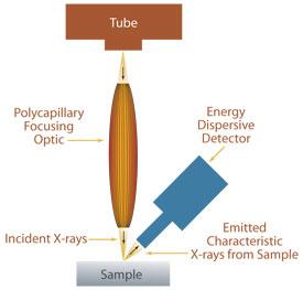 |
Fig.1. Standard MXRF configuration. A sample can be scanned to measure the elemental distribution with a spatial resolution as small as 10 �m (energy dependent).
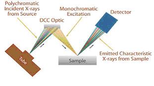 |
Fig.2. Monochromatic Micro EDXRF using Double Curved Crystal Optics. Doubly curved crystal optics directs an intense micron-sized monochromatic X-ray beam to the sample surface for enhanced elemental analysis.
Polycapillary focusing optics is capable to collect X-rays and focus the beam to diameters as small as tens of micrometers.
The MXRF systems are used for a wide range of applications, including archaeology, biology, contaminant identification, electronics defect identification, engine wear analysis, environmental analysis, forensic science, geology and metallurgy, jewelry, materials identification and control, micro and nanotechnologies, museums (for instance, restoration of art masterpieces), pharmaceutics, troubleshooting, etc.
Combined system AFM + MXRF from NT-MDT
Recently NT-MDT Company reported that their engineers together with the specialists from the Institute for Roentgen Optics are working on the design of a new and highly innovative system, which combines Atomic Force Microscope and Micro X-ray fluorescence module . This equipment will greatly enhance AFM capability by adding elemental identification as an option, which will be an important advance in the field of nanoscale instrumentation.
The integrated system (Fig.4) besides AFM includes X-ray tube with compact low voltage power supply, automatic multi-channel digital signal processor with dead- time correction and silicon drift detector (SDD -detector). MXRF module is compatible with any NTEGRA- platform based instrument. The combined system from NT-MDT for chemical elemental analysis offers several unique features.
First and major of them is the system integration approach that allows joining two research techniques in one device - the AFM and the MXRF. This 2-in-1 system is capable to obtain the topography of the surface and study the elemental composition of the same area of the specimen with high space resolution.
The second advantage of NT-MDTs system is provided by use of the Kumakhov X-ray polycapillary optics (X-ray lenses) in the MXRF design. This optics called micro structured optical arrays (MOA) is an instrument for focusing neutron beams and X-rays. MOA utilize total external reflection at grazing incidence from an array of small channels in order to reach maximal capture angle not exceeding certain critical value for incidence angle and to bring X-rays (neutron beams) to a common focus. Numerous reflections permit turning the beam to a total angle of several degrees. Any beam entering an empty smooth tube (for instance, a glass tube), with the angle of incidence smaller than critical angle, will be reflected numerous times from the inner surfaces of the tube. At the exit of this tube the "virtual" X-ray source will be formed. With such polycapillary system it is possible to focus the beam in the spot of various sizes. By applying this unique patented technology the specialists from the Institute for Roentgen Optics received the elemental spectra with a very small focal spot (down to 15 �m).
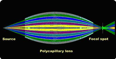 |
Fig.3. Polycapillary Kumakhov lens.
The third advantage of this system is provided by the specifics of the X-ray source. The source utilized in the MXRF module (Fig.5) has low capacity and low power, along with high intensity of energy at the surface of the object. The module is compact, lightweight, and has increased safety guaranteed.
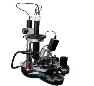 |
Fig.4. Combined system NTEGRA + MXRF
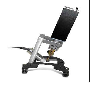 |
Fig.5. X-Ray Spectrometer MXRF module
The supporting experiment
The following is an experiment designed to demonstrate NT-MDT's MXRF module capability. The calibration grating SNG01 for a near-field scanning optical microscope (SNOM) was used as a sample. The SNOM grating represents a regular structure of vanadium film (10 nm thick) deposited on a quartz (SiO2) substrate.
The AFM scan of the sample obtained the topography of the object that clearly shows the areas with principal differences. In the AFM scan below there are distinctively visible diamond shaped structures representing the vanadium film deposited on the quartz substrate; the left part (see Fig.6) of the substrate didn't have any coating. Roentgen spectra were taken from both of these areas using the MXRF module.
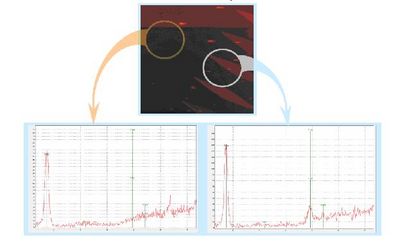 |
Fig.6. Supporting experiment configuration and results:Spectrum of quartz substrate (A); Spectrum of vanadium deposition (B) (image courtesy NT-MDT).
In spectrum A there is a single silicon characteristic peak with no vanadium peaks (see the green marker). The characteristic peak of vanadium is clearly seen in spectrum B (the green marker) as well as silicon peak that correlate with the sample structure. Technical parameters: 15 kV, 200 �A, beam size at the sample ~ 15 �m.
The NT-MDT mainstream in nanoinstrumentation design
As it was highlighted above, flexible nanotechnology equipment is useful for optimization of the processes control, defects discovery, quality management, which, in turn, might substantially increase the effectiveness at the nanoscale level. The challenge in the field of nanotechnology instrumentation is to design and implement new measurement techniques and standards to meet the needs of next-generation advanced manufacturing, which will rely on nanometer scale materials and technologies. At this moment the needs for measurement and characterization of new sample structures and characteristics far exceed the capabilities of current measurement science.
The more complex technology is introduced, the more sophisticated equipment is required. The anticipated advances in emerging nanotechnology may even require new type of metrology with higher resolution and accuracy than was envisioned before. So, it is of great importance these new metrology systems to be capable to determine and measure numerous physical and chemical
properties of nanostructures. The common feature of latest developments from NT-MDT is the combination of AFM with certain other advanced methods of research or control. These combined techniques allow receiving more detailed and versatile information about the object under study and, subsequently, greatly enhance the capability of the instrument and of the laboratory/production facility. In fact this is the primary goal of the company that is a pioneer in the field of integrated nanoinstruments.
Generally speaking, the mainstream of NT-MDT instruments design consists of two directions. The first one relates to development of a "smart" instrument for industrial applications. This type of highly sophisticated and automated devices includes numerous engineering ideas and user scenarios, but the operator uses only a few controls (at times only one button). The most powerful example of such system is Solver NEXT that received prestigious award from the R&D magazine in 2009 .
The goal of the second approach is integration of completely different scientific methods to accomplish multiple tasks in a single system. The NTEGRA platform was developed for this approach and allows such integrating of SPM with other instruments. The principle was materialized in NTEGRA Spectra (the integrated SPM and Raman spectrometer with its gigantic amplification of the Raman signal), which was awarded by the R&D Magazine as one of the 100 top solutions in 2006 .
The entirely new idea stands behind the novel design of the system that integrates the Scanning Probe Microscopy with Micro X-ray fluorescence spectrometry. This new system represents the first step on this way, but the NTEGRA platform is well suitable for such integration experiments. Overall, the prospective of such broad nanotechnology instrumentation strategy looks well defined and successful.
References:
G. Binnig, H. Rohrer (1986). "Scanning tunneling microscopy". IBM Journal of Research and Development 30: 4.
Steve Bunk. Better microscopes will be instrumental in nanotechnology development. Nature, 410, 127-129 (1 March 2001) | doi:10.1038/35065204
M Capitanio et al. FIONA in the trap: the advantages of combining optical tweezers and fluorescence. 2007 J. Opt. A: Pure Appl. Opt. 9 S157 doi: 10.1088/1464-4258/9/8/S07
S.S. Kharintsev, G.G. Hoffmann, J. Loos, G. de With, P.S. Dorozhkin, and M. Kh. Salakhov. Subwavelength-Resolution Near-Field Raman Spectroscopy. Journal of Experimental and Theoretical Physics, Vol. 105, 2007.
http://www.ntmdt.com/device/ntegra-solaris
http://www.ntmdt.com/device/ntegra-spectra
Instrumentation and Metrology for Nanotechnology. Report. National Nanotechnology Initiative workshop, NIST, 2004: www.nano.gov/NNI_Instrumentation_Metrology_rpt.pdf
Cheryl Blanchard. Atomic Force Microscopy. The chemical educator, 1996, Vol. 1, No. 5
X-ray fluorescence.Wikipedia: http://en.wikipedia.org/wiki/X-ray_fluorescence
Mattiuzzi, M. and Markowicz, A., 47th Annual Denver X-Ray Conference, paper F-41, 1998.
Spiller, E (2003). "X-Ray Optics". Encyclopedia of Optical Engineering: Taylor & Francis. doi:10.1081/E-EOE-120009497
Kumakhov, MA (1990). "Channeling of photons and new X-ray optics". Nuclear Instruments and Methods in Physics Research Section B 48, (1-4): 283--286. doi:10.1016/0168-583X(90)90123-C)
http://www.ntmdt.com/device/solver-next
http://www.rdmag.com/Awards/RD-100-Awards/R-D-100-Awards/
http://www.ntmdt.com/press-releases/view/our-ntegra-spectra-has-won-prestigious-r-d-100-award
Bookmark:


|
|
||
|
|
||
| The latest news from around the world, FREE | ||
|
|
||
|
|
||
| Premium Products | ||
|
|
||
|
Only the news you want to read!
Learn More |
||
|
|
||
|
Full-service, expert consulting
Learn More |
||
|
|
||