Home > Nanotechnology Columns > NanoGlobe > Nanotechnology has been identified as the key drive for technology innovation in Japan
 |
NanoGlobe Pte Ltd Nanotechnology Business Development Consultants NanoGlobe Pte Ltd |
Abstract:
Tsukuba innovation arena for nanotechnology (TIA nano) was launched on Feb 15th, 2010. AIST, NIMS and the University of Tsukuba are the 3 main operational partners of this national collaborative center that serves as a platform for industry-university-government cooperation and global partnership to promote nanotechnology innovation. During Feb 15-16th 2010, TIA Nanotech International Workshop was held at AIST. Invited speakers from world-leading nanotech centers/corporation such as MINATEC, NanoNed, SUNY at Albany, IBM, Intel, IMEC etc. shared their experience and provided recommendation to TIA nano on the cost-effective nanotech research center management, network and IP protection as well as the technical subjects in areas such as Nano-Electronics & Nanophotonics, N-MEMS, and Nanocharacterization.
May 6th, 2010
Nanotechnology has been identified as the key drive for technology innovation in Japan
Tsukuba city is a science city in Japan located with major national research institutes, a university, industry R&D laboratories, manufacturing companies. The National Institute of Advanced Industrial Science and Technology (AIST), National Institute for Materials Science (NIMS) and University of Tsukuba agreed to integrate their research capabilities and human resources to build a global center for nanotechnology innovation in Tsukuba, which is named as Tsukuba Innovation Arena for Nanotechnology (TIA nano). TIA nano is the largest nanotech initiative in Japan with a total investment of 500MUSD including 200M USD infrastructure and 300MUSD R&D funded by Japan Ministry of Economy, Trade and Industry (METI). An addition of 50MUSD funded by Ministry of Education, Culture, Sports, Science and Technology (MEXT) for infrastructure, and other extra funding from Tsukuba University specifically for education and training. "In collaboration with Tsukuba University, TIA Nano will launch the first International Nanotechnology Graduate School aiming at 50% overseas students and co-sponsored by major industries in the region such as Samsung, Hitachi and other multinational companies", shared by Mr. Tomosaburo Yano, Director for R&D Coordination from METI.
The mission of TIA nano is to function as an open innovation R&D center and to accelerate the commercialization of innovated nanotechnology in conjunction with education of the next generation. The nanotech center will have 3 core infrastructures including Nanodevice Research Foundry (45-65nm COMS & N-MEMS prototype device and 200-300mm wafer level fabrication and testing), Nanotech Open User Facilities (characterization, fabrication and processing) and Networking School of Nanotechnology (graduate school operated by University of Tsukuba and partner universities). To kick off the launch the nanotech center, TIA nano organized a 2 day workshop during Feb 15-16th 2010 at AIST and invited speakers from world-leading nanotech centers, consortiums and corporations including France MINATEC & LETI, Nanotechnology in The Netherlands (NanoNed), College of Nanoscale Science and Engineering at State University of New York at Albany (CNSE SUNY Albany), University of California Berkeley, IBM, Intel, Belgium IMEC, Canadian National Institute for Nanotechnology (NINT), US DOE Nanoscale Science Research Center - Center for Integrated Nanotechnology (CINT) & NIST, Germany Fraunhofer-Gesellschaft, Korea National NanoFab Center (NNFC) & Korean Research Institute of Standards and Science (KRISS) as well as Japan Nanonet, Tohoku University, University of Tokyo, Micromachine Center, AIST, Fujitsu.
We were most impressed by such a high level gathering of the world's top micro/nano-tech centers and were able to meet top scientists and center executives from all over the world at one place and learn about their world-class R&D activities, managing academia and industry cooperation, intellectual Property (IP), state of the art infrastructures and strategy for promoting open innovation and international collaboration. Special technical session focused on nanoelectronics and its integration with photonics. The purpose of the workshop intends to show case different business model of micro/nano-tech center/consortium in Europe, Asia and USA for TIA nano to figure out the best practice for its own operation. Click here for the program of this workshop.
MINATEC shares similar concept to TIA nano putting education, R&D and industry development under one roof.
Dr Bernard Meyerson, IBM Vice President for Strategic Alliances and CTO shared with the audience IBM global ecosystem strategy for advancing innovation and system solution provider business strategy, and stressed on building human resource and skills.
IMEC practices an open innovation system, co-ownership of foreground IP with its industry residents. "We stay out of the industry partner core business and focus on application driver at pre-competitive stage and not on the core business of our industry partner to avoid conflict of interest", Dr Chris Van Hoof (Director of Heterogeneous Integrated Microsystems) shared. IMEC R&D focuses on "must have areas" and builds a complete value chain (ecosystem) under one roof to ensure efficiency of operation. It also leverages university resources to make the R&D low cost, IMEC plays as a translator from university to industry. The presence of industry partner makes transfer implicit within IMEC. "We do not work with industry at a distance, we practice openness in evaluation and obtain immediate feedback on sites to improve efficiency and multiply efforts", Dr Van Hoof emphasized.
Dr Paolo Gargini from Intel indicated "The killer application is the Interactive Digital Media (IDM) for nanoelectronics enabling young generation communication (socioeconomics)".
"Science and Engineering is a preferred major for Asian students especially in the developing world where young people are very hungry and motivated. TIA nano could tap into the Asia young talent as well as the hungry SMEs and entrepreneurs national and internationally to accelerate its R&D progress and commercialization development", Dr Lerwen Liu, Managing Director suggested.
In the closing remarks, Dr Toshihiro Matsui (Program Director of AIST) concluded, "TIA nano will serve as a collaborative platform for nanotechnology innovation by integrated 3 core infrastructures and 6 core research areas and enhance the industry-university-government cooperation as well as global partnerships, especially in the fields of Green-IT and basic research to enable quantum leaps in nanotechnology".
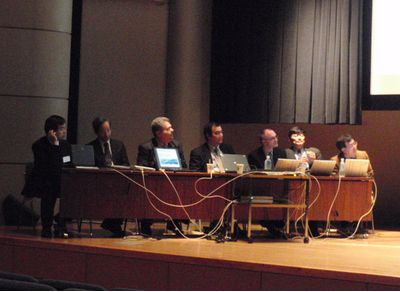 |
| Figure 1. Panel Discussion on what are the most effective ways to develop nanoelectronics for what application areas. From left to right: Dr Naoki Yokoyama (Fujitsu), Prof. Yasuhiko Arakawa (Univ. of Tokyo), Dr Bernard S Meyerson (IBM), Dr Paolo Gargini (ITRS(Intel)), Dr Chris Van Hoof (IMEC), Dr Makoto Hirayama (SUNY Albany) and Dr Toyohiro Chikyow (NIMS) |
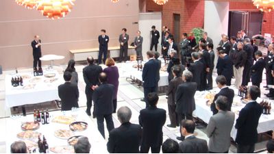 |
| Figure 2. Workshop welcome dinner on Day 1 |
Bookmark:


|
|
||
|
|
||
| The latest news from around the world, FREE | ||
|
|
||
|
|
||
| Premium Products | ||
|
|
||
|
Only the news you want to read!
Learn More |
||
|
|
||
|
Full-service, expert consulting
Learn More |
||
|
|
||