Home > Nanotechnology Columns > NanoNewsNet.ru > Flux growth of GaN is challenging epitaxy: Russian scientists rush with the new technology
 |
Eugene Birger Principal Analyst NanoNewsNet.ru |
Abstract:
The new method of GaN monocrystal structures fabrication with extremely low spatial defect frequency.
July 14th, 2009
Flux growth of GaN is challenging epitaxy: Russian scientists rush with the new technology
The development of LEDs (light emitting diodes) based products is a very promising direction for investments due to high rates of market growth. The LEDs based lighting products are capable to substitute the traditional light sources, such as incandescent, fluorescent and other lamps. Using the light emitting diodes will significantly reduce the consumption of electric power and simplify lighting systems' operation. It will also free up quite an amount of power capacity.
Recently, RUSNANO, ONEXIM and the Ural Optical and Mechanical Plant established the joint company to manufacture the new generation lighting products ("see here": http://en.rusnano.com/Publication.aspx?PublicationId=1072 ). This project is aimed at creating a highly technological industrial production of a new generation lighting systems based on the gallium nitride (GaN) semiconductor chips. The final product will be LED chips, LED lamps and lighting systems, the brightness of which is comparable with the best world analogues. The record low amount of defects in semiconductor layers would allow these devices to work without losing effectiveness with high-density currents, enabling the good brightness to price ratio for LED chips.
It is not well known that the Nanotechnology Group at South Ural State University in Chelyabinsk had developed a new and very effective method for GaN crystals growing them from the flux.
Very special physical, chemical and electrical properties of gallium nitride make it ideal material for the blue and ultraviolet solid-state lasers/laser diodes and sensors that could be useful and effective in photonics, communications, digital devices, power electric grids, RGB displays etc. It's high chemical and temperature stability makes this material very valuable for defense and aerospace applications. GaN monocrystal would be an excellent substarte for epitaxial GaN films build-up - and by analogy with the silicon monocrystals, it could be used for multilayer electronic chips manufacturing (diodes, transistors, etc). Unfortunately, lack of practical methods for fabricating monocristals of gallium nitride prevents wide industrial applications of this material.
Traditionally the high crystalline quality GaN for blue LEDs are fabricated using the low temperature vapor phase epitaxial growth on heterosubstartes (usually sapphire). The difference in the properties (for instance, in coefficients of thermal expansion) between the deposited layer and the substarte leads to numerous cracks during the cooling off phase. Gallium nitride compounds tend to have a high spatial defect frequency, on the order of a hundred million to ten billion defects per square centimeter. It dramatically decreases it's performance characteristics. The best LEDs have less than 2 years of continuous luminescence.
The new method is offering the fabrication of GaN monocrystal structures with extremely low spatial defect frequency (small experimental quantities manufactured in the lab show only 100 defects per square centimeter).
By this time the largest GaN crystals ( the plates 10-20 mm wide and 0.1-0.2 mm thick) had been grown just from a Na/Ga flux held under 30-50 atm pressure of N2 at 750 -800 oC (USA, Japan) or from molten pure gallium (1000-5000 atm и 1300-1500�С). These results highlight the perspectives of this method.
The major technical problem, which stands in the way of this technique - the congruent GaN melting occurs under 60000 atm of N2 pressure at 2200�С. Fortunately there are the ways to dissolve gallium nitride in suitable melt.
The solubility plays the critical role in forming GaN crystals. The GaN solubility in liquid Na at 750-850�С does not exceed 0.1%. The dilution of melted GaN by the elements that form fusible ion nitrides alloys (for instance Li) and at the same time form fusible double nitrides (Li3GaN2 etc) allows dramatically increase the solubility of GaN in such a molten alloy.
Unfortunately, there is a new and serious problem here - not only high temperatures and pressures, but also the proper selection of materials for container need to be researched. Very aggressive additions (Li, Li3N) that intensify the crystal growth, at the same time dissolve not only the GaN, but the other materials as well (corundum, graphite, boron nitride, platinum, etc). The new research - to find more resistant materials is needed. Recently several teams from various centers are investigating the new systems with Ga and nitrogen to discover the full picture of GaN monocrystals formation. The research of two or more alloying components simultaneous influence, which looks promising, was not systematic, but is important to learn how to control the monocrystals properties.
The South Ural State University scientists led by d-r Dmitry Zherebtsov set up numerous autoclave experiments to grow GaN monocrystals in various conditions, which allowed them to select the most perspective direction. Set of GaN flux grown samples were prepared in WC, ZrB2, pyrolithic BN, hot pressed BN, nitrided Gd, Nb and Al2O3 crucibles covered with steel or Stainless Steel (SS) lid or with another crucible bottom to reduce Na evaporation. The typical volume of the melt was 1-2 cm3, typical temperature, pressure, and dwelling time 800-850 �C, 50 atm N2 and 100-200 h. Starting compositions vary in Na, Li, Ga, C content. Several samples were grown with addition of NaCl, KCN or Na2CN2. For some samples starting atmosphere was doped with 0.3-2 g of NH3 gas or crucible contained 0.2-1 g pieces of metals (Ta, W, La, Gd, Er) or BN.
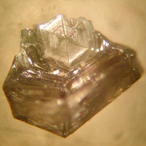
Currently the scientists are able to fabricate 1-2 mm crystals, and they are very optimistic about the way for potential size increase. Resulted crystals were brown, yellowish, gray, greenish or white; normally the higher Li content the less coloration. After extracting from the furnace the samples were washed consequently with ethanol, water, aqua regia and distilled water. Powder X-ray diffraction patterns confirmed single phase GaN with highly ordered crystal lattice for all samples.
The Ural researchers work in collaboration with their colleagues from Germany and Finland. Currently the team is in talks with St. Petersburg's Ioffe Physical-Technical Institute of the Russian Academy of Sciences - one of Russia's largest research centers specialized in physics and technology about joint research. The new technology is able successfully complement traditional epitaxial techniques by fabricating the substrates of excellent quality and size.
 |
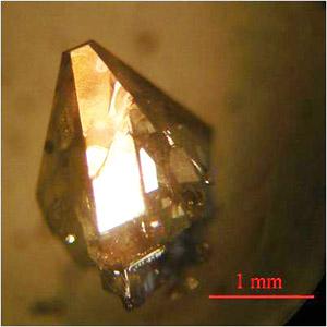 |
Prism and pyramid shape GaN crystals fabricated in South Ural State University's lab.
Ural chemists say that similar research programs exist in Japan, Korea, China, Poland, and USA, but currently Russian results are more advanced. To win the competition they need 3 years and some financing.
Project Economics
Picky and thorough Ural researchers say they need about three more years to develop experimental industrial technology. By the end of third year (with the project fully financed) according to the estimates they would be able to produce 2-3 kg of 50-100 g high quality crystals per month. During the next two years they plan to build an industrial prototype with the throughput 10-15 kg 100-150 g crystals per month. Expected production cost to be about $20,000-$30,000 per 1 kg of GaN.
Eugene Birger
1-707-849-7824
Bookmark:


|
|
||
|
|
||
| The latest news from around the world, FREE | ||
|
|
||
|
|
||
| Premium Products | ||
|
|
||
|
Only the news you want to read!
Learn More |
||
|
|
||
|
Full-service, expert consulting
Learn More |
||
|
|
||