Home > Nanotechnology Columns > Bo Varga > New Nano Solar Developments in 2009
 |
Bo Varga Managing Director Silicon Valley Nano Ventures |
Abstract:
Nanotechnology can reduce costs, increase performance, and lower the environmental impacts of solar PV and CSP. Every month I read about nanotechnology impacts on solar photovoltaics and talk with start up / early stage companies and I am amazed and impressed by the many different and interesting research projects that report results. And by many new commercialization efforts, although I am often under NDA and cannot discuss those.
This column reports on a few developments over the last year with a particular focus on the increasing interest in nanocrystalline-based solar cells and on the use of Schottky barrier/junction approaches to increase solar cell efficiency. As well as on the use of Schottky junctions to replace p:n type solar cells with "perfect diode" based solar cells.
June 22nd, 2009
New Nano Solar Developments in 2009
Nanotechnology Solar Photovoltaic Developments June 2009
For a very interesting read on the importance of replacing coal, gas, and oil as fuel sources, a just-released study of sea levels and atmospheric CO2 predicts that CURRENT
atmospheric levels will lead to 25 meters (82 feet) rise in sea levels. Based on current resistance in China, EU, USA to actually change business as usual - and what do we do about cement, steel, and methane from cows, and etc. humans will not stop the rise of atmospheric CO2 levels any time soon.
http://www.sciencecentric.com/news/article.php?q=09062103-study-documents-close-relationship-between-past-warming-sea-level-rise
Editorial: I constantly hear about "solar subsidies" and "grid parity" and am always amazed by the disinformation spread by old energy industries.
Coal, gas, oil mining, drilling, and use are all heavily subsidized, both directly and indirectly. Direct subsidies include explicitly granted rights to destroy the land in West Virginia by coal mining, the depletion allowance for gas and oil extraction, rights of way for pipelines granted by government action via eminent domain, etc. Indirect subsidies include global warming as well as asthma, cancer, and other health effects, reduced crop, forest, and fishery yields, etc.
All industrialized countries today trade human health and environmental destruction for cheap gasoline, cheap plastics, etc. As for grid parity there is no absolute number. Where I live in Silicon Valley my electricity bill for a family of three is in the 30 cents/KWH grid power cost level by the second week of each month - and we have no airconditioning and do not heat or cook with electricity. On a lifetime real cost basis, including cradle to cradle costing, I will argue that solar PV and certainly CSP is cheaper today than coal, gas, or oil - whenever industrial populations decide the destroying the environment and human health is not a good tradeoff then the monetary cost for power from coal, oil, and gas will exceed solar.
A simple solution is to put a carbon tax and a health tax and a drilling/mining environmental restoration tax on coal, oil, gas. But we would have to give up cheap gasoline, cheap tourism, cheap and high fat and high salt foods, low cost plastics, and other gains that today are considered much more important by most business interest groups than healthy people in a healthy environment.
Editorial Ends Here
Nanotechnology can reduce costs, increase performance, and lower the environmental impacts of solar PV and CSP. Every month I read about nanotechnology impacts on solar photovoltaics and talk with start up / early stage companies and I am amazed and impressed by the many different and interesting research projects that report results. And by many new commercialization efforts, although I am often under NDA and cannot discuss those.
This column reports on a few developments over the last year with a particular focus on the increasing interest in nanocrystalline-based solar cells and on the use of Schottky barrier/junction approaches to increase solar cell efficiency. As well as on the use of Schottky junctions to replace p:n type solar cells with "perfect diode" based solar cells.
And a brief note - silicon prices are no longer an issue with all the new capacity coming on line and the collapse of global semiconductor markets, check out sources such as http://www.greentechmedia.com or http://www.luxreasearch.com . So any and all business plans and technologies that address the "high price of solar silicon" are very unlikely to get any investor interest. Companies such as TSMC (50% of global semiconductor sales of $20 billion in 2008) do not expect a recovery before 2012. We expect to see a number of new thin film technologies commercialized by 2012 and a large surplus of solar silicon.
http://en.wikipedia.org/wiki/Schottky_barrier "A Schottky barrier, named after Walter H. Schottky, is a potential barrier formed at a metal-semiconductor junction which has rectifying characteristics, suitable for use as a diode. The largest differences between an Schottky barrier and a p-n junction are its typically lower junction voltage, and decreased (almost nonexistent) depletion width in the metal. . . Schottky barriers, with their lower junction voltage, find application where a device better approximating an ideal diode is desired."
For those of us who took college physics years ago, a diode essentially permits current flow in only one direction http://en.wikipedia.org/wiki/Diode and lower junction voltage and decreased depletion width enable greater efficiency in electron transfer. After talking with researchers at Lawrence Berkeley National Labs a quick search http://patft.uspto.gov/ lists 11 patents using "solar" and "schottky" in title search:
1 5,155,565 Method for manufacturing an amorphous silicon thin film solar cell and Schottky diode on a common substrate
2 4,427,840 Plastic Schottky barrier solar cells
3 4,321,099 Method of fabricating Schottky barrier solar cell
4 4,278,830 Schottky barrier solar cell
5 4,227,943 Schottky barrier solar cell
6 4,215,185 Liquid junction schottky barrier solar cell
7 4,213,798 Tellurium schottky barrier contact for amorphous silicon solar cells
8 4,200,473 Amorphous silicon Schottky barrier solar cells incorporating a thin insulating layer and a thin doped layer
9 4,163,677 Schottky barrier amorphous silicon solar cell with thin doped region adjacent metal Schottky barrier
10 4,105,470 Dye-sensitized Schottky barrier solar cells
11 4,053,918 High voltage, high current Schottky barrier solar cell
and an additional 9 patents are listed when the same search terms are used in the abstract search:
12 6,674,064 Method and system for performance improvement of photodetectors and solar cells
13 4,544,797 Method for preventing short-circuits or shunts in a large area thin film solar cell and cell obtained thereby
14 4,395,583 Optimized back contact for solar cells
15 4,245,386 Method of manufacturing a solar cell battery
16 4,190,950 Dye-sensitized solar cells
174,167,015 Cermet layer for amorphous silicon solar cells
184,135,290 Method for fabricating solar cells having integrated collector grids
19 4,131,486 Back wall solar cell
20 4,104,084 Solar cells having integral collector grids
and an additional 5 patent applications are listed as published using the same search terms in an abstract search:
1 20090139763 Terminal box for a solar cell panel
2 20070289627 Nanoscale solar cell with vertical and lateral junctions
3 20060208653 Circuit improvements for solar lamps
4 20040092094 Integrated device technology using a buried power buss for major device and circuit advantages
5 20040074533 Superconductor-semiconductor solar cells and light detectors
In my next column I will review these patents, assignees (owners), and the possible role in future developments in solar PV. Even granted patents, however, do not guarantee a commercial, industrial scale application. We cannot repeat often enough that manufacturability and manufacturing economics is the key to making money on solar photovoltaics. And that field lives of devices need to be in the 20-year range for many applications. And that revenue is less than a hundred dollars per square foot versus a hundred dollars per square inch for many computer chips.
It is important to keep in mind that many research laboratories do not have the equipment, process control, or manufacturing skills to optimize solar cell performance (obvious exceptions include the Institute of Energy Conversion, University of Delaware - http://www.udel.edu/iec/ ) so the focus is often on relative improvement in efficiency and potentially lower or much lower materials or manufacturing costs. Commercial products based on these technologies often yield much higher conversion efficiencies.
But lab scientists can be unrealistic about the time required to commercialize technical breakthroughs that require process changes or developments including new manufacturing equipment. And that new technologies have to compete with the continued incremental improvements in the existing commercial technologies today - mono and polycrystalline wafer-based solar cells, amorphous crystal - one, two, or three absorber layers, and CdTe thin films - dominated today by First Solar but with companies such as Abound (formerly AVA Solar) and Primestar building their first commercial manufacturing lines). As well as CIGS where larger scale manufacturing looks possible in 2010.
In February the National Institute of Nanotechnology, Edmonton, Alberta, reported a significant step in improving the efficiency of nano-polymer solar cells, whose efficiency is limited by electron/hole recombination. This research shows an initial improvement on the order of 50% for the target interface in the device stack. What I found particularly interesting was the increase in efficiency was achieved by what looks like a decrease in the ordered structures that enables more efficient charge transfer.
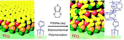 |
| Improved Plastic Solar Cell |
Title: Thienylsilance-Modified Indium Tin Oxide as an Anodic Interface in Polymer/Fullerene Solar Cells, (Feb 25, 2099 edition, ACS Applied Materials + Interfaces).
"The power conversion efficiency (η) of devices fabricated with thienylsilane-modified anodes (η) 1.5%) was found to be greater than for control samples prepared under identical conditions without surface-modified substrates (η) 1.0%)."
Another interesting development is the lead selenide nano crystal photovoltaic cells report in March 2009 on work done at NREL consists of a Ca/Al backside Schottky barrier, a PbSe NC (Nanocrystal) film, and ITO front contact on float glass. This is a very simple device stack with potentially a very low manufactured cost. As this device stack exhibits multiple exciton generation it is an example of a generation 3 photovoltaic device.
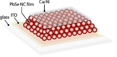 |
| Nano Crystal Schottky Solar Cell |
http://www.coloradocollaboratory.org/pdfs/45_midgett-semonin_abstract.pdf
"MULTIPLE EXCITON GENERATION, CHARGE CARRIER DYNAMICS, AND SOLAR ENERGY CONVERSION IN ELECTRONICALLY COUPLED FILMS OF PBSE NANOCRYSTALS
Multiple exciton generation (MEG) is a process that occurs in semiconductor nanocrystals where one highly energetic photon produces multiple charge carriers and can significantly enhance solar energy conversion efficiencies. Recently, we have developed a simple, ITO/PbSe-NC/metal cell via an Schottky junction at the back electrode that routinely produces a large short-circuit photocurrent and solar conversion efficiencies of ~ 2%. In this cell, the PbSe NC films are chemically treated using 1,2-ethandithiol (EDT) to produce highly photoconductive films that yield EQEs of 65% across the visible and up to 25% in the infrared region of the solar spectrum, with IQEs approaching 90%."
Clearly there is significant possibility for improvement in this approach to solar PV from the present conversion efficiency. Using 50% as the solar power in the visible spectrum, 65% EQE and 90% IQE yields a possible conversion efficiency of ~ 29%.
One interesting project at Lawrence Berkeley National Labs is using a combination of surface plasmon resonance I mentioned in prior columns to generate hot electrons and then an Schottky barrier to harvest electrons.
The claimed advantages for this technology include the use of abundant, low cost materials, simple cell design, and compatibility with various deposition technologies - http://www.lbl.gov/Tech-Transfer/techs/lbnl2195.html
ABSTRACT: "Third-generation" PV technologies are being actively pursued in academic research labs. These include nano-optics, multi-junction architectures, multi-exciton, plasmonics, and lower cost tandem cells. The goal is a module cost of less than $0.60/watt. Many of these technologies are in exploratory or early research stages but still can be evaluated according to their material requirements, processing complexity, and potential scalability. For example, concepts that utilize GaAs or CIGS may have cost issues or material availability issues. Similarly, complex cell designs or designs that feature nano-architectures such as quantum wires may not be easily scaled.
Robert Kostecki and Sam Mao of Berkeley Lab have invented a new approach to affordable, third generation PV. The technology builds upon previous research that uses surface chemical reactions to generate and inject hot electrons into a metal catalyst. In the recent invention, light is absorbed by the PV material and hot electrons are generated. Charges are then separated across a Schottky barrier.
The technology is a simple, low cost, scalable solution that addresses the concerns of high cost materials, materials availability and toxicity, complexity of cell design, and large-scale manufacturability. It relies on cheap, abundant materials that do not require ultra-high purity processing. Various existing deposition technologies can be used for cell manufacturing, none of which rely on ultra-high vacuum or expensive MOCVD/MBE equipment.
Based on the initial laboratory conceptual demonstration, greater than 10% efficiency is projected with process development on existing tool sets. The technology uses a simple cell design that, together with the processing flexibility, should provide a path to scalable manufacturing."
Unfortunately the PCT application graphic is too low resolution to reproduce well for this column, however you can see the device structure by following the link; the actual device structure is quite simple, with nano scale Ag as the SPR material generating hot electrons and a nano scale TiO2 absorber layer.
Moving more to the industrial side Konarka Power Plastics - www.konarka.com - announced an addition $45 million in equity funding for a 20% stake in the company with Total Gas and Power, one of the largest publicly-traded integrated international oil and gas companies in the world. This brings the total investment in Konarka to $150 million with an additional $20 million in government research grants.
After 7 years in development of organic photovoltaic technology, Konarka released commercial Power Plastic in 2008 and opened a Gigawatt (1,000 MW) nameplate a manufacturing plant. The company's focus from founding is on using low cost plastics for the top and bottom layers of solar cells manufactured using roll-to-roll (R2R) printing and coating technologies.
The promise is very low cost materials and manufacturing, the issues are field life (polymer bonds degrade in sunlight) and efficiency - a 6% efficient cell was announced last December by University of California, Santa Barbara and Universit� Laval researchers. Key technical innovations include the photo-reactive polymer material invented by Konarka co-founder and Nobel Prize winner, Dr. Alan Heeger, and the device stacks, manufacturing process, and application devices developed over the past 8 years by industrial partners - Konarka only makes and sells the power plastic materials that other companies integrate into end user products.
While there has been a lot of skepticism expressed over the past few years about nanotechnology based startup companies in general and Konarka specifically, it now appears this company has achieved takeoff after resolving many difficult technical and business issues.
Moving to a company that is still in early stage mode, Solexant, www.solexant.com - closed a B funding round of $18+ million last Fall when the financial markets were in free fall - a very strong vote of confidence for a company that raised a $4+ million A round in August, 2007. A review of the company's web site that lists Dr. Paul Alivisatos as a board of directors member and then backtracking to the Lawrence Berkeley National Labs (where Dr. Alivisatos is currently the acting director) gives us a good idea of where this company is heading in commercializing nanocrystalline solar PV.
An October 20, 2005 press release first described the breakthrough nanotechnology - http://www.lbl.gov/Science-Articles/Archive/MSD-nanocrystal-solar-cells.html - Researchers with Berkeley Lab and the University of California, Berkeley, have developed the first ultra-thin solar cells comprised entirely of inorganic nanocrystals and spin-cast from solution. These dual nanocrystal solar cells are as cheap and easy to make as solar cells made from organic polymers and offer the added advantage of being stable in air because they contain no organic materials.
"Our colloidal inorganic nanocrystals share all of the primary advantages of organics � scalable and controlled synthesis, an ability to be processed in solution, and a decreased sensitivity to substitutional doping - while retaining the broadband absorption and superior transport properties of traditional photovoltaic semiconductors," said Ilan Gur, a researcher in Berkeley Lab's Materials Sciences Division.
The researchers describe a technique whereby rod-shaped nanometer-sized crystals of two semiconductors, cadmium-selenide (CdSe) and cadmium-telluride (CdTe), were synthesized separately and then dissolved in solution and spin-cast onto a conductive glass substrate. The resulting films, which were about 1,000 times thinner than a human hair, displayed efficiencies for converting sunlight to electricity of about 3 percent. This is comparable to the conversion efficiencies of the best organic solar cells, but still substantially lower than conventional silicon solar cell thin films.
"We obviously still have a long way to go in terms of energy conversion efficiency," said Gur, "but our dual nanocrystal solar cells are ultra-thin and solution-processed, which means they retain the cost-reduction potential that has made organic cells so attractive vis-�-vis their conventional semiconductor counterparts."
With the stunning financial success of First Solar after launching their first commercial PV module manufacturing plant in 2004, CdTe has grown in popularity, especially with the financial community. And First Solar has current manufacturing costs of 93 cents/WP - while the next closest technology, a-Si, costs $1.50/WP for the most efficient manufacturers. So the promise of new CdTe based solar PV technologies has great attraction for investors.
Further information on Dr. Alivisatos' solar technologies can be seen by searching under his name at http://www.lbl.gov/Tech-Transfer/techs/index.html#Environment .
Another interesting set of nano + solar technologies have been developed by Dr. Zettl and Dr. Grossman and are listed below:
�High-Efficiency, Self-Concentrating Nanoscale Solar Cell
" the invention makes it possible to design even higher efficiency solar cell devices made of conventional materials, such as silicon, cadmium-tellurium, indium-gallium-nitrogen, or cadmium-selenium. . . . photonic nanocrystals can be customized to function as any one of a number of parts of a functioning solar cell all within a single nanoscale unit. These parts include a photovoltaic region that converts sunlight into electricity; a photonic crystal area that reflects and absorbs light; or a sophisticated, nanoscale wavelength sorter that pairs wavelengths with a coupler tuned to the desired frequency. This ability to sort wavelengths of incoming sunlight makes it possible for the broadband-capable device to self-focus within a specific range of wavelengths and to capture and use photons that would otherwise not be utilized by a standard solar cell."
�Ideal Configuration for Nanoscale Solar Cells
"The standard design of excitonic solar cells, which includes most organic-based solar cells, is ideal in only two out of three dimensions. In other words, excitons can diffuse vertically and not reach a contact. Moreover, because the structure of real blended systems is less regular than the ideal structure, other problems that limit device performance arise, such as shorting and interface electronics.
Berkeley Lab researchers Alex Zettl and Jeffrey C. Grossman have invented a configuration and method for making an exciton-based photovoltaic cell that overcomes this problem. By using a controlled repeating structure, excitons interface in all three dimensions to minimize exciton recombination and maximize photovoltaic conversion efficiency. "
�Controlled Structure of Organic-Nanomaterial Solar Cells
"Organic, polymer-based solar cells--lightweight alternatives to conventional, silicon-based solar cells--have great potential for delivering inexpensive solar energy and lowering manufacturing costs while maintaining high power efficiency. However, the highest efficiency achieved so far with polymer-based solar cells is only 5% to 6% . . . the synthesis of these solar cells is controlled only by temperature and mixing times; yet neither factor adequately controls the structure of nanofeatures, such as conductive channels, that play a significant role in solar cell performance.
. . . controlling the molecular shape, structure, and pattern of the materials in organic, polymer-based solar cells . . . improves power efficiencies by a factor of two. The new method provides a way to make affordable, high-performance, polymer-based solar cells as well as optoelectronic devices (LEDs, nanolasers) and light collectors.
To ensure that conductive channels are grown in the direction most suitable for efficient charge extraction, magnetic or electric fields are used to align magnetically-doped semiconductor nanoparticles as they are blended with photovoltaic materials. This creates a well-controlled interface or connection between the solar cell's components and overcomes a common hurdle in standard polymer-based solar cells--the internal loss of electronic charges before they can usefully exit the device. As a result, photons can be more efficiently absorbed and converted to energy."
And for a last and very interesting technology, promising 35% conversion efficiency at the same cost as standard mono-Si or poly-Si solar cells, see:
.Low Cost, High Efficiency Tandem Silicon Solar Cells
"Wladek Walukiewicz, Joel Ager, and Kin Man Yu of Berkeley Lab have developed high-efficiency solar cells that leverage the well-established design and manufacturing technology of silicon cells while delivering the performance previously achievable only by far more complex and expensive tandem solar cells. The Berkeley Lab tandem solar cells are composed, in one configuration, of silicon and indium gallium nitride, creating a natural near-zero resistance tunnel junction without requiring doping.
The power conversion efficiency of multi-crystalline silicon solar cells is currently about 15 percent and that of the best single crystalline cells is 23 percent. The Berkeley Lab tandem silicon solar cells promise power conversion efficiencies of up to 35 percent, with manufacturing costs that are not significantly higher than those of simple multi or single crystalline silicon cells. While three junction non-silicon tandem solar cells have achieved unconcentrated efficiencies of up to 33%, the costs are prohibitive for wide-spread adoption. "
In summary, there are many new solar PV developments driven by nanotechnology R&D. Commercializing these technologies on a mass production scale always takes more time and money than initially estimated. In the current financial climate the $100+ million required to bring a new solar PV technology to mass production is a serious barrier to entry. Possible paths to commercialization for a start up / early stage company include licensing mass production to large manufacturers such as TSMC, which claimed 50% of global semiconductor sales of $20 billion, or Intel, or Samsung.
Please send your feedback, ideas, and suggestions to .
Bo's focus is on the commercialization of technology via consulting and transactions-focused marketing to close business deals, funding, and people recruitment. Bo has 30 years experience developing business strategy, funding, & strategic alliances for start-up and early stage companies in Silicon Valley & globally. He has 8 years experience with the commercialization of nano technology & clean technology ventures, with a primary focus on advanced nano-materials, solar energy, batteries, & water.
Current projects include nano-improved coatings, rubber, paints, "soil glue", and several water treatment / remediation projects, all of which have some commercial traction, a diesel pollution solution, and a new solar thermal company seeking to penetrate California and USA markets.
Bookmark:


|
|
||
|
|
||
| The latest news from around the world, FREE | ||
|
|
||
|
|
||
| Premium Products | ||
|
|
||
|
Only the news you want to read!
Learn More |
||
|
|
||
|
Full-service, expert consulting
Learn More |
||
|
|
||