Home > Nanotechnology Columns > Bo Varga > Commercialization of Nano + Solar Photovoltaic Technologies
 |
Bo Varga Managing Director Silicon Valley Nano Ventures |
Abstract:
This column focuses on issues of interest to entrepreneurs, investors, and researchers in the nano + solar space; (1) listing of some of upcoming conferences relevant to nano + solar (2) overview of commercial considerations for any nano + solar technology (3) overview of some key technologies currently in early stages of commercialization. In my early July column I will review all the new nanotechnologies and companies related to solar that are announced in the year ending June 30, 2008 - and there are many.
May 9th, 2008
Commercialization of Nano + Solar Photovoltaic Technologies
Nanotechnology & Solar Power: May 2008
This column runs monthly and focuses on nanotechnology + solar PV conferences, commercialization, companies, fundings, issues, and technology. All quotations and sources are referenced and all opinions are the opinions of the columnist & not of Nanotechnology-Now.
To my many readers I apologize for the delay in updating you on nanotechnology impacts on more efficient and/or lower cost solar photovoltaic (PV) cells and panels. I am committed to publish another three to four columns this year and appreciate feedback regarding your interests.
We all know that the solar market is hot - growing at some 40% per annum as far as the analyst can project (we have completed projections through 2020, some publicly available reports project to 2025). And most of us know that current solar technologies have a long way to go to achieve "grid parity" electricity production costs or efficiencies in converting photons to electrons at the 68% - 74% theoretical efficiency levels cited by Dr. Martin Green of the University of New South Wales, see slide 17 in an excellent PDF file available on-line that covers current state of the art and the future http://www.tvworldwide.com/events/eqtv/061016/ppt/Martin%20Green.pdf
I should note my own bias in favor of thin film solar PV versus silicon wafer-based solar PV. And a mild bias in favor of Silicon versus more exotic materials. The materials cost and manufacturing cost of thin-film solar is much lower than wafer based and drops much faster than wafer based in large-scale manufacturing. Thin film solar PV appears today to be the only manufacturing approach that can reach "grid parity" levels in the next decade, that is, the same cost for electricity as you pay your electrical utility. And in the long run the supply of Silicon is essentially unlimited, while the supply of Indium, Gallium, and Tellurium has significant limits if Solar is to replace coal, oil, and gas for electricity generation.
I will address three topics in this column that should be of interest to entrepreneurs, investors, and researchers in the nano + solar space; (1) listing of some of upcoming conferences relevant to nano + solar (2) overview of commercial considerations for any nano + solar technology (3) overview of some key technologies currently in early stages of commercialization. In my next column I will review all the new nanotechnologies and companies related to solar that are announced in the year ending June 30, 2008 - and there are many.
(1) Conferences: attending the following conferences will give you access to a wide range of companies, entrepreneurs, technologies, and investors in the nano + solar space. A brief note - nanotechnology enables clean energy / solar and, while solar conferences do not stress the nano theme, many of the companies that present utilize nano to achieve targeted price and performance on nano + solar products.
The 33rd Annual IEEE Photovoltaics Specialists Conference will be held in San Diego on April 11-16, see http://www.33pvsc.org/public/ for more information. This is a technical conference and we are particularly interested in subject Area 2: CIGS, II-VI, and Related Thin-Film Cells and Technologies. William N. Shafarman of the Institute of Energy Conversion/University of Delaware chairs this area. The IEC/UD is a world-class research center that achieved the highest efficiency solar cell in 2007 of 42.9% by using a beam splitting technology and then optimizing a different solar cell material for each of three chunks of the solar spectrum - see http://www.udel.edu/iec/Publications/DARPA_22nd_EUPVSEC.pdf
The IEEE Area 2 will present recent advances in the processing and device fabrication, characterization, and modeling of Cu(InxGa1-x)Se2, CdTe, and other thin-film PV materials including thin-film deposition, microstructure characterization, electrically active defects, role of impurities such as Na in CIGS or Cl in CdTe, novel device structures and their characterization, and reliability. In addition paper on advanced manufacturing processes, the influence of grain boundaries, alternative buffer layers and TCOs, and tandem cells will be presented.
As we stress later, solar PV is all about manufacturing! Nano just adds more time and money cost to bring up a new, economical manufacturing process.
The NanoEquity Asia 2008 Conference will be held in Singapore, May 28-29. This is a business conference, see http://www.nano-globe.biz/nanoequity08/edm2b and a number of the presenting companies and organizations are involved in solar PV.
Clean Tech2008, held in conjunction with www.nsti.org Nano2008 conference in Boston from June 1 to 5 will present a range of start-up/early stage companies in the Solar Technologies & Applications space, see http://www.csievents.org/Cleantech2008/ the Nano2008 conference, in turn, is the world's most important and largest nano technology conference. The Nano conference is in its' 11th year and is a must attend for nano technologists. As a West Coast resident I appreciate the fact that the Nano conference alternates each year between coasts and will be held on the West coast in 2010. Clean Tech2008 is a business conference while Nano2008 is both a business and a technical conference.
Intersolar North America 2008 http://www.intersolar.us/ will be held July 15-17 in San Francisco, in conjunction with SemiconWest, the annual trade show for the semiconductor industry. Intersolar Europe is the largest PV trade show in Europe with 40,000 visitors expected in Munich June 12-14. This first US event for Intersolar is a trade event focused on the North American and global solar markets, and our primary purpose in attending is to meet with companies that have actual products in the market today and to determine where nano plays a role - materials, coatings, etc.
Solar Power 2008 is the most rapidly growing and largest US solar trade show and will be held in San Diego October 13-16. This is an industry and business conference with especially strong participation from Asian countries. We will present more information in our next column. This conference is a "must" for people in the US interested in solar, see http://www.solarpowerconference.com/ for more details.
(2) Commercial considerations are becoming more important globally for nano + solar as funding sources increasingly want to commercialize their investments in research. In our experience the same issues need to be addressed when evaluating an interesting technology with great potential based on laboratory / science experiment results.
Professional funding sources in general - corporate, private equity, and venture capital - do not want to fund science or science experiments. Rather they want to fund the engineering development required to achieve commercially viable products. A commercially viable product is a product that can compete successfully in the marketplace 3, 5, 7 etc. years downstream when the new "wonder" product sells in high volumes at a good enough gross margin to yields a profitable return on investment. Ideally a very profitable return on investment.
With correct (or lucky) market timing, investors will realize an extraordinary return from the new technology company they have funded, often through 3, 4, or 5 investment rounds. This extraordinary return via an IPO or sale or merger of the technology company is required to balance out investments in other technology companies that result in a loss of all or part of the investment. And to justify the often long and painful path a technology company requires to achieve positive cash flow and profitability.
In the case of a new nano + solar technology company, for example, an investment of $100+ million over 3 to 5 years is typical, often this money and time is required to achieve the first year of operating revenue. Even when an investor is considering an investment of $1 million in a start-up company, the real consideration is whether that company merits and investment of $100 million!
In prior columns we have mentioned the stage gate process for evaluating investments in technology commercialization & product development, see http://www.stage-gate.com/ and from an investor/management point of view the following are the major stages in technology commercialization.
The value of technology increases significantly at each stage, assuming success at each stage. And so does the investment in commercialization, often a 10x increase at each move from stage to stage.
We start with a "lab phenomena", that is some material, device, or process shows interesting results. Next we see a "proof of concept" where the lab phenomena focused on a commercial idea, such as a nano + solar coating material. Next we see a product prototype, ideally focused on product requirements as specified by a prospective customer. Then we see an alpha product, often used as an in-house development platform for a beta product, which in turn is tested by prospective customers and results in a commercial product after required modifications.
This is a typical process for a material, component, or device and each step takes time.
And in the case of solar manufacturing considerations play a major role, which most scientists and research-oriented engineers often do not take into consideration. Commercializing new technologies often requires new manufacturing processes where capital expense for the design, development, and manufacture of new equipment, material cost (especially for tightly specified nano materials), processing cost (especially energy inputs), and throughput (yield of good solar panels at the targeted efficiency levels). When we engage in due diligence on a new nano + solar technology we always start with the best possible current estimate for capital expense (fixed cost), materials and processing cost (variable cost), and throughput for specified product.
The volume selling price and variable and allocated fixed expense per solar panel are the key measures to determine if commercializing a nano + solar technology makes economic sense.
Typical times and investments for successful nano + solar project that start with a proof of concept are 18 months post $5 - $10 million funding to achieve a product prototype and an in-line manufacturing process, another 18 months post $25 - $50 million funding to build and commission a pilot manufacturing plant, and another 18 months post $70 - $120 million funding to build and commission an economical scale manufacturing plant (with enough throughput to generate enough revenue and profit to justify the investment).
From our research (our solar team includes very strong manufacturing, device, project development, and finance experts) the ideal manufacturing process from a cost, throughput, and scalability point of view would be to deposit a single absorber layer on a large substrate at a high speed, for example drum coating inks in a roll-to-roll process (R2R) where the absorber layer is based on "one pot synthesis" of optimal size distribution quantum dots which "magically" self assemble from small sizes at the top of the layer to absorb ultra-violet, high energy photons through a gradation down to the lowest layer where the largest sizes self-locate to absorb the far infrared, low energy photons. Ideally this same single layer leverages the multiple-exciton effect (see NREL roadmap paper referenced below, so that high energy photons set off a multiple electron cascade that can be harvested for maximum conversion efficiency.
(3) Key technologies tend to focus on reducing cost and/or increasing efficiency of solar PV cells and modules. While nano can be of value in the electronic components of solar PV, such as inverters, diodes, etc. our knowledge base and experience is much stronger in the thin film technology, device stack, and manufacturing area.
Thin film solar PV was first commercialized by ECD/Ovonics who pioneered the amorphous-silicon (a-Si) technology, which today has the major share of the thin film PV market, see http://www.ovonic.com/eb_so_solar_overview.cfm . Companies today can purchase turnkey a-Si manufacturing plants from Applied Materials in the US, Oerlikon in Switzerland, or Ulvac in Japan, among others.
There are four other thin film technologies; cadmium telluride (CdTe) to date successfully commercialized only by First Solar, with AVA Solar and Primestar/GE expected to be in commercial production in 2009; copper indium sulfide/copper indium gallium diselenide (CIS/CIGS) with many players either ramping production, Daystar, Nanosolar, Honda, etc. or just starting production; various organic technologies, and various nano-based technologies.
While ALL thin film technologies depend upon nano-scale coatings to be effective and require manufacturing control at the nano level, our area of interest is in a-Si related technologies and also in specific nano based thin film PV.
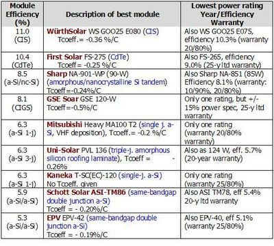
As can be seen by a review of the efficiency of current thin film commercial vendors, see http://www.nrel.gov/pv/thin_film/pn_techinfo_latest_updates.html and the "Best Commercial Module Efficiencies" spreadsheet and "Commercial Module Efficiencies Survey" table, from which I extracted the thin film vendors listed below.
 |
| Solar Module (Panel) Efficiencies April, 2008 |
Note Tcoefficient = loss of efficiency from 20 C with every 1 C rise in temperature, for more information please see: http://photovoltaics.sandia.gov/docs/PDF/IEDFB5~1.pdf
This data is gathered from the various solar PV vendor's web sites and is based on the actual guaranteed performance. As my readers can see, the best current a-Si modules (solar panels) range in efficiency from 5.3% to 6.3% in actual use and after "burn in" and Sharp's dual junction (two photon absorber layers) solar panels which have a nano-crystalline top absorber layer achieve 8.5% efficiency at an increase in cost. First Solar's very successful CdTe panels (the lowest manufactured cost per Watt/Peak (Wp - standard unit of measure for rating solar panels) is 10.4%, and the two CIS/CIG vendors listed, GSE Solar and W�rthSolar warranty 8.1% and 11% respectively.
(3) Key technologies work to address the gap between actual solar technologies commercialized today and the potential efficiencies of solar panels. The difference between the 5.3% - 11% efficiencies available today and the 42.9% cell developed at the IEC/UC and the 68%-74% theoretical efficiency based on thermodynamic principles show a major gap that various nano-technology companies and researchers are working to fill.
We are only at the beginning of solar cell technology commercialization.
I project a doubling of efficiencies in the next decade with no increase in cost per Wp, which in turn implies no increase in fixed cost (equipment) or variable cost (materials & energy).
I hope I am a pessimist but faced with the real challenges of moving from the "proof of concept" to the large scale manufacturing process, the next generation technologies that will be commercialized in 2012-2017 time framework will very likely come from companies that began in the 2006-2008 period.
More details regarding the challenges facing solar PV development are available as individual reports published June, 2007 under the "National Solar Technology Roadmap" . I have included the titles and links below in quotes, which are a "must read" for entrepreneurs, investors, and researchers interested in the commercialization of solar PV. For general link for all publications see:
http://www1.eere.energy.gov/solar/solar_america/publications.html#technology_roadmaps
"Technology Roadmaps (from NREL)
Ten photovoltaic (PV) technology roadmaps were developed in 2007 by staff at the National Renewable Energy Laboratory (NREL), Sandia National Laboratories, U.S. Department of Energy (DOE), and experts from universities and private industry. This work was done, in part, to support activities within the Solar America Initiative.
� Wafer-Silicon PV (PDF 341 KB)
� Film-Silicon PV (PDF 363 KB)
� Concentrator PV (PDF 304 KB)
� CdTe PV (PDF 286 KB)
� CIGS PV (PDF 327 KB)
� Organic PV (PDF 260 KB)
� Sensitized Solar Cells (PDF 297 KB)
� Intermediate-Band PV (PDF 287 KB)
� Multiple-Exciton-Generation PV (PDF 292 KB)
� Nano-Architecture PV (PDF 265 KB)"
Three major limiting factors for the efficiency of a-Si based solar PV (the dominant thin film technology today and for the next decade) are: (i) limited bandwidth absorption of the solar spectrum, particularly in the infra-red, about 45% of all insolation at sea level; (ii) limited capture of photons due to "bounce back" from the thin absorber layers, typically 200 nanometers thick; and (iii) irregular grain size and grain boundaries result in limited capture of photons and high recombination of electrons and holes generated by the PV effect.
Technologies and companies addressing these problems include for (1) all companies listed in the table above using double and triple junction (absorber layer) device architectures, as well as startups such as www.solexant.com and major turnkey solar PV factory providers such as Applied Materials, Oerlikon, and Ulvac that are using nano crystalline silicon or other nano materials; and for (ii) companies focused on using thin film manufacturing methods but increasing the thickness of the absorber layer, this technology is just being commercialized by startups as well as established companies such as http://www.nanogram.com/?p=solar that are commercializing methods to rapidly deposit thick films - 10 microns to 35 microns and using a mono crystal seed layer to convert silane gases (used in standard a-Si thin film solar PV manufacturing) into mono crystalline solar PV panels; and finally for(iii) start-up companies such as www.aossolar.com (where we are business strategy and marketing consultants) that target recrystallization of a-Si to poly-crystalline solar PV panels to achieve the economics of high throughput thin film solar PV manufacturing with the efficiencies of crystalline silicon solar panels, currently in the 13.3% to 19.3% efficiency range.
A nano technology that we believe has a great future is the use of nano particles as an absorber/emitter layer on the top of a thin film solar PV panel, where most of the preliminary research is being conducted on an a-Si platform. Thin films have the problem of limited capture of photons - they tend to bounce out of the absorber layer - and current methods such as anti-reflection coatings and rough back surfaces have limited success in keeping photons in the planar surface. Research by people such as Dr. Edwin Yu at the University of San Diego, http://nanolab.ucsd.edu/ety/ , has shown a 10%-15% increase in solar cell efficiency and simulations indicate the potential for a 50% increase in efficiency. The main problem with this approach is manufacturing - the optimal deposition of the optimal size nano materials at a low cost and high throughput. We are currently talking with a company (under NDA) regarding a solution to this problem and expect to be able to cover this technology in our next column.
Another nanotechnology that we believe has a great future is the use of meta-materials, that is materials whose properties depend on their structure, particularly revelant to 3-D nanomaterials. While initial applications for 3-D nanomaterials have been in coatings and membranes (fuel cells, water purification, etc.) meta-materials have the potential to capture and target the solar spectrum to achieve very high efficiency levels.
We are in dialog (under NDA) with a start-up company that has achieved maximum solar cell conversion efficiencies (in the laboratory only) and are currently exploring the technical and manufacturing roadmaps to achieving an economical solar panel.
Given the many challenges to be overcome, especially volume manufacturing and low cost, we do not expect to see a solar panel utilizing metamaterials to be available before 2015-2020.
A good overview as well as a listing of research groups on this topic, as well as some recent papers and portals are at: http://en.wikipedia.org/wiki/Metamaterial . For several good web portals, see: http://www.metamorphose-vi.org/ and also http://www.metamaterials.net/ .
Our next column, published in early July, will cover relevant nanotechnologies in detail as well as some of the companies working to commercialize these technologies.
Final Note: Some readers may find this column to be too simplistic while others may find this column to be too technical. We have bandwidth to answer your questions. Please send your feedback, ideas, and suggestions to My focus is on business development and marketing based on 29 years experience developing business strategy, funding, & strategic alliances for start-up and early stage companies in Silicon Valley & globally. I have 7 years experience with the commercialization of nano technology & clean technology ventures, with a primary focus on solar energy, batteries, & water. Recent work is focused on helping nano + energy companies develop business and market strategies and acquire funding, as well due diligence for investors regarding new technologies & projects in the thin film solar PV, e.g. a recently completed due diligence report for investors for a new solar PV manufacturing process/plant to be funded at the $130 million level.
Bookmark:


|
|
||
|
|
||
| The latest news from around the world, FREE | ||
|
|
||
|
|
||
| Premium Products | ||
|
|
||
|
Only the news you want to read!
Learn More |
||
|
|
||
|
Full-service, expert consulting
Learn More |
||
|
|
||