Home > News > Old Company Press Releases > Purdue News
Nanoparticles Could Aid Biohazard Detection, Computer Industry
West Lafayette, Ind. December 11th, 2002
A group led by Jillian Buriak has found a rapid and cost-effective method of
forming tiny particles of high-purity metals on the surface of advanced
semiconductor materials such as gallium arsenide. While the economic
benefits alone of such a discovery would be good news to chip manufacturers,
who face the problem of connecting increasingly tiny computer chips with
macro-sized components, the group has taken their research a step further.
The scientists also have learned how to use these nanoparticles as a bridge
to connect the chips with organic molecules. Biosensors based on this
development could lead to advances in the war on terrorism.
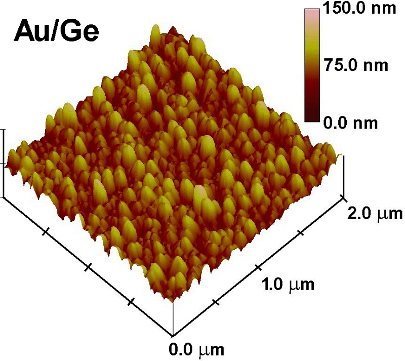
Click to enlarge A micrograph image of gold nanoparticles form on germanium, an advanced semiconductor material. These tiny particles could create better connections between microchips and the much larger wires that lead to other computer components. (Graphic/Lon Porter) |

Click to enlarge Nanoparticles form gradually after a semiconductor is dipped into a solution of metal salt. The cycle progresses from a surface of bare germanium (at the 12 o'clock position) progressing clockwise to the same surface 500 minutes after immersion. The process occurs naturally, without the expensive equipment that is otherwise necessary to produce high-purity metals. (Graphic/Lon Porter) |
"We have found a way to connect the interior of a computer with the
biological world," said Buriak, associate professor of chemistry in Purdue's
School of Science. "It is possible that this discovery will enable chips
similar to those found in computers to detect biohazards such as bacteria,
nerve gas or other chemical agents."
The research, which appears in today's (Wednesday, 12/11) issue of Nano
Letters, sprang from the team's desire to attach metals to semiconductors in
precise locations.
Computer chips, commonly made of silicon, contain circuits that are far
smaller than those made from metal wires. But for an impulse from a keyboard
or mouse to reach the microchip, the electronic signal must pass from a
large wire onto the chip's surface. The delicate interface between the macro
and micro world is often accomplished by a tiny connection made of gold,
chosen frequently over alternatives such as copper or silver, because it
does not corrode in air. Gold's advantages have made it the first choice for
designers, though until now such advantages have come at a steep economic
price.
"Gold works great once you actually get it onto the chip," said Lon Porter,
a chemistry graduate student in Buriak's group. "But by traditional
manufacturing methods you need to begin with expensive, very high-purity
gold. With our method, however, you'd no longer need the high-quality gold
you might find in coins in Fort Knox - you could use the low-purity gold
waste swept up from the coin factory floor."
In their purest forms, precious metals such as gold and platinum are among
the most coveted substances in the world. But these metals are more commonly
found in nature as part of low-purity compounds like metal salts - which,
despite their name, are not salts you would use to flavor food or make a
snowy roadway safe for driving. The amount of precious metals in these salts
is low to begin with; when the salts are dissolved in liquid at the
concentration that Buriak's group needs to form nanoparticles, a test tube
full of the solution is worth only pennies. But despite the low market value
of the chemical solutions themselves, the effect Buriak's group has
discovered may nonetheless prove to be a gold mine.
"All you need to do to form nanoparticles is dip the semiconductor into the
solution and wait," Porter said. "Though you begin with a solution worth
less than the change in your pocket, you still end up with a layer of gold
nanoparticles on the silicon that has the same purity as gold bullion.
Because the reaction sustains itself, manufacturers would not need any
special training or equipment to use it. From both a manpower and a
technical perspective, the process is a real money saver."
The particles grow larger with increased time in the solution and eventually
cover the semiconductor base with a bumpy coating. The roughness of the
coating gives the base a greater surface area than it had by itself, a
realization which led to the team's second breakthrough.
"It's similar to the way your brain packs a lot of surface area into the
limited space inside your skull by folding in on itself many times," Porter
said. "But the advantage we found for computer chips is not that we can
increase their 'thinking power,' per se. Rather, the resulting rough surface
gives us a lot of nooks and crannies in which to secure a second group of
molecules atop the gold - organic molecules that react in the presence of
other chemicals."
The upshot of this double-layering is that the organic molecules could be
chosen for their ability to react to the presence of nerve gas or biological
contaminants. If a dangerous chemical reacted with an organic molecule, the
metal nanoparticles could convey a signal downward to the chip that a
biohazard was present.
"When a chemical reaction takes place, a small but measurable electrical
change takes place," Porter said. "As metals are excellent conductors of
electricity, nanoparticles could be the bridge that we need to make
computers interface with the biological world."
Further refinement of their techniques has allowed the group to deposit
nanoparticles of gold, platinum and other metals in specific areas of the
semiconductor's surface. Rather than a film that blankets the entire
surface, the group can deposit the particles in a grid pattern or even draw
lines with a microscopic "pen." These refinements could allow manufacturers
to put their discoveries to use comparatively rapidly.
"We are not sure what application of our discoveries will appear first,"
Buriak said. "But there are many semiconductor companies out there that
spend a lot of money on chip interfacing, and we expect they could all take
advantage of this technique somehow."
This research was funded in part by the National Science Foundation.
Buriak's group is affiliated with Purdue's new Birck Nanotechnology Center,
scheduled for completion in the fall of 2004. A dozen groups associated with
the center are pursuing research topics such as microscopic machines,
advanced materials and artificial organs.
Writer: Chad Boutin, (765) 494-2081, cboutin@Purdue.edu
Sources: Jillian M. Buriak
Lon A. Porter Jr., (765) 496-3491, porterjr@Purdue.edu
Related Web sites:
Birck Nanotechnology CenterFor further information, please contact:
Jeanne Norberg, director
Purdue University News Service
400 Centennial Mall Drive, Room 324
West Lafayette IN 47907-2016
Office: (765) 494-2096; Fax: (765) 494-0401
Pager: (765) 423-8662; Cell: (765) 491-1460
Home: (765) 449-4986
jnorberg@Purdue.edu
http://news.uns.Purdue.edu
Reprinted with premission.
Copyright Purdue University.
If you have a comment, please
us.
|
|
||
|
|
||
| The latest news from around the world, FREE | ||
|
|
||
|
|
||
| Premium Products | ||
|
|
||
|
Only the news you want to read!
Learn More |
||
|
|
||
|
Full-service, expert consulting
Learn More |
||
|
|
||