Our NanoNews Digest Sponsors

Home > Nanotechnology Art Gallery > University of Cambridge - Department of Materials Science and Metallurgy
University of Cambridge - Department of Materials Science and Metallurgy
Click image to enlarge. All images © respective artist, university, or company. You must get permission from each source prior to using any of these images (Nanotechnology Now cannot grant permission).
To learn more about and to see more of these images, check out the following pages:
- University of Cambridge Department of Materials Science & Metallurgy Gallery
- Dr. Rafal E. Dunin-Borkowski: Awards
To learn more about some of the underlying research, visit
Dr. Rafal Dunin-Borkowski's work-related web pages.
Magnetic Nanotubes
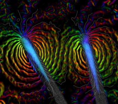
The nanotubes were fabricated in the University of Cambridge Engineering department by Yasuhiko Hayashi, who grew them using a Cobalt-Palladium catalyst. This alloy remains present in the ends of the nanotubes, and is magnetic. The nanotubes you see here have a 70-100nm diameter. Characterisation of the magnetic properties was carried out by Ed Simpson and Takeshi Kasama using Electron Holography, a TEM technique which records the phase of an electron wave. The phase, being affected by any magnetic field the electron passes through, therefore records any information on the magnetic properties on the sample under investigation. From this, the magnetic induction maps you see here can be generated. The colours represent the direction and intensity of the field, and the contours, the magnetic field lines. It is an entirely quantitative technique, so as well as these images of the field, the magnetic moment, for instance, can be deduced too.
|
Magnetic field of an iron crystal inside a carbon nanotube
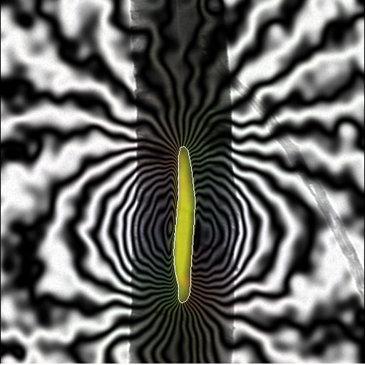
This image won First Prize in the "Science Close-Up" category in the Daily Telegraph Visions of Science competition. The image shows a multi-walled carbon nanotube, approximately 190nm in diameter, containing a 35-nm-diameter iron crystal encapsulated inside it. Electron holography has been used to obtain a map of the magnetic field surrounding the iron particle, at a spatial resolution of approximately 5nm. The magnetic phase contours show that the particle contains a single magnetic domain. An external magnetic field could be applied to such particles to exert a torque on the surrounding nanotube.
|
Crystal Kaleidoscope
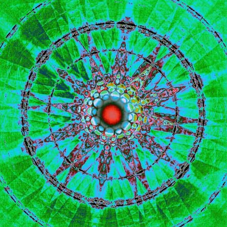
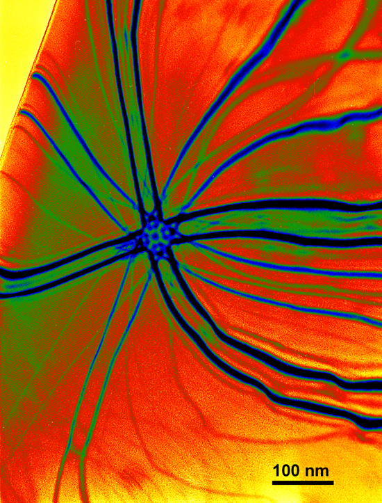
This is a false colour convergent beam electron diffraction pattern recorded at 150kV parallel to the three-fold axis of lanthanum aluminate. In addition to the mesh of reflections at the centre, the pattern also shows concentric circles of reflections in successive higher order Laue zones. Odd numbered zones have only a single branch of intensity that corresponds to scattering solely from the oxygen atoms in the structure.
|
Magnetic Rock

The image shows the magnetic microstructure in a natural, finely exsolved intergrowth of magnetite blocks in an ulvospinel matrix, which is influenced both by the shapes of the individual magnetite blocks and by magnetostatic interactions between them. Different colours correspond to different directions of magnetic induction in the sample.
|
Magnetic domains in a thin cobalt film

The colours in the image show the different directions of the magnetic field in a layer of polycrystalline cobalt that has a thickness of only 20nm. The direction of the magnetic field in the film changes at the positions of domain walls. The field of view is approximately 200�m. The image was acquired using the Fresnel mode of Lorentz microscopy in a field emission gun transmission electron microscope. It was recorded out of focus to enhance the contrast of the domain walls, and then converted to a colour induction map by applying the Transport of Intensity Equation to the image intensity.
|
Magnetic field lines in a bacterial cell
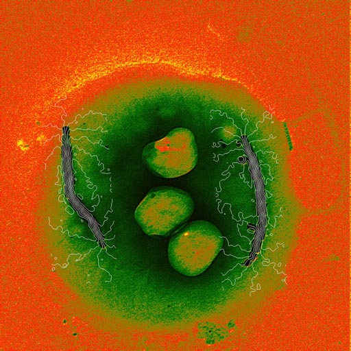
The image shows the magnetic field lines in a single bacterial cell. The fine white lines are the magnetic field lines in the cell, which were measured using off-axis electron holography. Such bacteria live in sediments and bodies of water, and move parallel to geomagnetic field lines as a result of the torque exerted on their magnetosome chains by the earth's magnetic field.
|
Magnetic field lines around an iron wire

The image shows magnetic field lines around the end of an iron wire, which is magnetized along its length. The field of view is approximately 1�m. The image was acquired using electron holography in a field emission gun transmission electron microscope.
|
'Dancing' quantum dot
Plan view bright field transmission electron micrograph of a germanium/silicon quantum dot in a silicon matrix. The quantum dot, grown by molecular beam epitaxy, is coherently strained due to Ge/Si crystal lattice mismatches giving rise to strain induced banding contours. The straight edge at the top left shows the Si 110 plane. Field of view is approximately 620nm wide.
|
Yttrium barium copper oxide 'dragonflies'
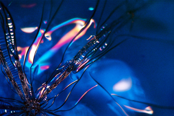
Internal structure of yttrium barium copper oxide (YBCO) ink, prepared by sol-gel methods. The superconducting YBCO ink is jet-printed onto the substrate. Cracking occurs when the stable YBCO ink dries too quickly, giving this 'dragonfly' effect. Image taken by optical microscopy. Diagonal length of image approximately 125 microns.
|
|
|
||
|
|
||
| The latest news from around the world, FREE | ||
|
|
||
|
|
||
| Premium Products | ||
|
|
||
|
Only the news you want to read!
Learn More |
||
|
|
||
|
Full-service, expert consulting
Learn More |
||
|
|
||