Home > Press > Graphene grows – and we can see it
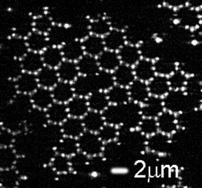 |
| Pieces of a graphene lattice made from patchy particles. Because the particles can be followed one-by-one, defects can be studied at the particle scale. Image: Swinkels et al. CREDIT Swinkels et al |
Abstract:
Graphene is the strongest of all materials. On top of that, it is exceptionally good at conducting heat and electrical currents, making it one of the most special and versatile materials we know. For all these reasons, the discovery of graphene was awarded the Nobel Prize in Physics in 2010. Yet, many properties of the material and its cousins are still poorly understood – for the simple reason that the atoms they are made up of are very difficult to observe. A team of researchers from the University of Amsterdam and New York University have now found a surprising way to solve this issue.
Graphene grows – and we can see it
Amsterdam, Netherlands | Posted on March 24th, 2023Two-dimensional materials, consisting of a hyper-thin single layer of atomic crystal, have attracted a lot of attention recently. This well-deserved attention is mainly due to their unusual properties, very different from their three-dimensional ‘bulk’ counterparts. Graphene, the most famous representative, and many other two-dimensional materials, are nowadays researched intensely in the laboratory. Perhaps surprisingly, crucial to the special properties of these materials are defects, locations where the crystal structure is not perfect. There, the ordered arrangement of the layer of atoms is disturbed and the coordination of atoms changes locally.
Visualizing atoms
Despite the fact that defects have been shown to be crucial for a material’s properties, and they are almost always either present or added on purpose, not much is known about how they form and how they evolve in time. The reason for this is simple: atoms are just too small and move too fast to directly follow them.
In an effort to make the defects in graphene-like materials observable, the team of researchers, from the UvA-Institute of Physics and New York University, found a way to build micrometre-size models of atomic graphene. To achieve this, they used so-called 'patchy particles’. These particles – large enough to be easily visible in a microscope, yet small enough to reproduce many of the properties of actual atoms – interact with the same coordination as atoms in graphene, and form the same structure. The researchers built a model system and used it to obtain insight into defects, their formation and evolution with time. Their results were published in Nature Communications this week.
Building graphene
Graphene is made up of carbon atoms that each have three neighbours, arranged in the well-known ‘honeycomb’ structure. It is this special structure that lends graphene its unique mechanical and electronic properties. To achieve the same structure in their model, the researchers used tiny particles made of polystyrene, decorated with three even tinier patches of a material known as 3-(trimethoxysilyl)propyl – or TPM for short. The configuration of the TPM patches mimicked the coordination of carbon atoms in the graphene lattice. The researchers then made the patches attractive so that the particles could form bonds with each other, again in analogy with the carbon atoms in graphene.
After being left alone for a few hours, when observed under a microscope the ‘mock carbon’ particles turned out to indeed arrange themselves into a honeycomb lattice. The researchers then looked in more detail at defects in the model graphene lattice. They observed that also in this respect the model worked: it showed characteristic defect motifs that are also known from atomic graphene. Contrary to real graphene, the direct observation and long formation time of the model now allowed the physicists to follow these defects from the very start of their formation, up to the integration into the lattice.
Unexpected results
The new look at the growth of graphene-like materials immediately led to new knowledge about these two-dimensional structures. Unexpectedly, the researchers found that the most common type of defect already forms in the very initial stages of growth, when the lattice is not yet established. They also observed how the lattice mismatch is then ‘repaired’ by another defect, leading to a stable defect configuration, which either remains or only very slowly heals further to a more perfect lattice.
Thus, the model system not only allows to rebuild the graphene lattice on a larger scale for all sorts of applications, but the direct observations also allow insights into atomic dynamics in this class of materials. As defects are central to the properties of all atomically thin materials, these direct observations in model systems help further engineer the atomic counterparts, for example for applications in ultra-lightweight materials and optical and electronic devices.
####
For more information, please click here
Contacts:
Laura Erdtsieck
Universiteit van Amsterdam
Office: 0031-205-252-695
Copyright © Universiteit van Amsterdam
If you have a comment, please Contact us.Issuers of news releases, not 7th Wave, Inc. or Nanotechnology Now, are solely responsible for the accuracy of the content.
Bookmark:


| Related Links |
| Related News Press |
News and information
![]() Simulating magnetization in a Heisenberg quantum spin chain April 5th, 2024
Simulating magnetization in a Heisenberg quantum spin chain April 5th, 2024
![]() NRL charters Navy’s quantum inertial navigation path to reduce drift April 5th, 2024
NRL charters Navy’s quantum inertial navigation path to reduce drift April 5th, 2024
![]() Discovery points path to flash-like memory for storing qubits: Rice find could hasten development of nonvolatile quantum memory April 5th, 2024
Discovery points path to flash-like memory for storing qubits: Rice find could hasten development of nonvolatile quantum memory April 5th, 2024
2 Dimensional Materials
![]() NRL discovers two-dimensional waveguides February 16th, 2024
NRL discovers two-dimensional waveguides February 16th, 2024
Graphene/ Graphite
![]() NRL discovers two-dimensional waveguides February 16th, 2024
NRL discovers two-dimensional waveguides February 16th, 2024
Possible Futures
![]() Discovery points path to flash-like memory for storing qubits: Rice find could hasten development of nonvolatile quantum memory April 5th, 2024
Discovery points path to flash-like memory for storing qubits: Rice find could hasten development of nonvolatile quantum memory April 5th, 2024
![]() With VECSELs towards the quantum internet Fraunhofer: IAF achieves record output power with VECSEL for quantum frequency converters April 5th, 2024
With VECSELs towards the quantum internet Fraunhofer: IAF achieves record output power with VECSEL for quantum frequency converters April 5th, 2024
Chip Technology
![]() Discovery points path to flash-like memory for storing qubits: Rice find could hasten development of nonvolatile quantum memory April 5th, 2024
Discovery points path to flash-like memory for storing qubits: Rice find could hasten development of nonvolatile quantum memory April 5th, 2024
![]() Utilizing palladium for addressing contact issues of buried oxide thin film transistors April 5th, 2024
Utilizing palladium for addressing contact issues of buried oxide thin film transistors April 5th, 2024
![]() HKUST researchers develop new integration technique for efficient coupling of III-V and silicon February 16th, 2024
HKUST researchers develop new integration technique for efficient coupling of III-V and silicon February 16th, 2024
Discoveries
![]() Chemical reactions can scramble quantum information as well as black holes April 5th, 2024
Chemical reactions can scramble quantum information as well as black holes April 5th, 2024
![]() New micromaterial releases nanoparticles that selectively destroy cancer cells April 5th, 2024
New micromaterial releases nanoparticles that selectively destroy cancer cells April 5th, 2024
![]() Utilizing palladium for addressing contact issues of buried oxide thin film transistors April 5th, 2024
Utilizing palladium for addressing contact issues of buried oxide thin film transistors April 5th, 2024
Materials/Metamaterials/Magnetoresistance
![]() Nanoscale CL thermometry with lanthanide-doped heavy-metal oxide in TEM March 8th, 2024
Nanoscale CL thermometry with lanthanide-doped heavy-metal oxide in TEM March 8th, 2024
![]() Focused ion beam technology: A single tool for a wide range of applications January 12th, 2024
Focused ion beam technology: A single tool for a wide range of applications January 12th, 2024
Announcements
![]() NRL charters Navy’s quantum inertial navigation path to reduce drift April 5th, 2024
NRL charters Navy’s quantum inertial navigation path to reduce drift April 5th, 2024
![]() Discovery points path to flash-like memory for storing qubits: Rice find could hasten development of nonvolatile quantum memory April 5th, 2024
Discovery points path to flash-like memory for storing qubits: Rice find could hasten development of nonvolatile quantum memory April 5th, 2024
Interviews/Book Reviews/Essays/Reports/Podcasts/Journals/White papers/Posters
![]() Simulating magnetization in a Heisenberg quantum spin chain April 5th, 2024
Simulating magnetization in a Heisenberg quantum spin chain April 5th, 2024
![]() Discovery points path to flash-like memory for storing qubits: Rice find could hasten development of nonvolatile quantum memory April 5th, 2024
Discovery points path to flash-like memory for storing qubits: Rice find could hasten development of nonvolatile quantum memory April 5th, 2024
|
|
||
|
|
||
| The latest news from around the world, FREE | ||
|
|
||
|
|
||
| Premium Products | ||
|
|
||
|
Only the news you want to read!
Learn More |
||
|
|
||
|
Full-service, expert consulting
Learn More |
||
|
|
||