Home > Press > JEOL Introduces New Scanning Electron Microscope with “Simple SEM” Automation and Live Elemental and 3D Analysis
 |
Abstract:
A new Scanning Electron Microscope (SEM) from JEOL answers the need for faster and easier acquisition of both SEM images and EDS data analysis, especially suited for repetitive operations and quality control.
JEOL Introduces New Scanning Electron Microscope with “Simple SEM” Automation and Live Elemental and 3D Analysis
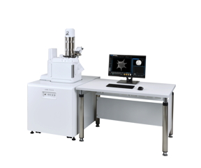
Peabody, MA | Posted on January 14th, 2022JEOL, the global leader in the development of cutting-edge Electron Microscopes for materials characterization and analysis, introduces its latest SEM, the JSM-IT510. This new Scanning Electron Microscope features productivity enhancing automation, including “Simple SEM” automated imaging, automated montaging (both image and EDS map) and live EDS analysis (spectrum and map).
The IT510 is the successor to the popular JEOL IT500 InTouchScope SEM, with its large sample chamber and tungsten or LaB6 filament. The IT510 features JEOL Intelligent Technology that enables seamless navigation from optical to SEM imaging, Live EDS and 3D analysis, and auto functions from alignment to focus for fast, clear, and sharp images.
The user of the new IT510 has several productivity-enhancing new features:
The new Simple SEM function automates image collection at multiple locations on a sample, and sets the various conditions required, including magnification and settings. Simple SEM simplifies and automates workflow for routine tasks.
A new “Live 3D” function constructs 3D images of the sample surface during observation showing surface shape and depth information in real time.
A Signal Depth automated function calculates the X-ray generation depth to support understanding of the analytical spatial resolution within a specimen under the conditions set. Useful when conducting elemental analysis.
A new Low-vacuum Hybrid Secondary Electron Detector collects both electron and photon signals, providing an image with high S/N and enhanced topographic information. This detector also supports photon imaging with specimens that give a cathodoluminescence response.
Live Mapping displays the elemental map simultaneously with SEM imaging, made possible by a new Integrated SEM and Energy Dispersive X-ray Spectrometer (EDS) System. The user can switch seamlessly between the live map view and spectrum view during SEM image observation. Then they can overlay the element maps of interest on the live SEM image for enhancing understanding of element distribution within a specimen.
Zeromag software seamlessly navigates to the area of interest from an optical image of a larger general area of the sample. The user is never lost and can easily navigate to the desired observation area by simply clicking on the optical image.
The JEOL IT510 is designed for unprecedented ease-of-use with advanced SEM technology in a compact platform. This smart-flexible-powerful Scanning Electron Microscope delivers the highest level of intelligent technology with built-in automation for the most versatile analytical SEM available today.
####
For more information, please click here
Contacts:
Pamela Mansfield
Marketing Communications
JEOL USA
11 Dearborn Road
Peabody, MA 01930
978-536-2309
Copyright © JEOL USA
If you have a comment, please Contact us.Issuers of news releases, not 7th Wave, Inc. or Nanotechnology Now, are solely responsible for the accuracy of the content.
Bookmark:


| Related News Press |
News and information
![]() Simulating magnetization in a Heisenberg quantum spin chain April 5th, 2024
Simulating magnetization in a Heisenberg quantum spin chain April 5th, 2024
![]() NRL charters Navy’s quantum inertial navigation path to reduce drift April 5th, 2024
NRL charters Navy’s quantum inertial navigation path to reduce drift April 5th, 2024
![]() Discovery points path to flash-like memory for storing qubits: Rice find could hasten development of nonvolatile quantum memory April 5th, 2024
Discovery points path to flash-like memory for storing qubits: Rice find could hasten development of nonvolatile quantum memory April 5th, 2024
Imaging
![]() Nanoscale CL thermometry with lanthanide-doped heavy-metal oxide in TEM March 8th, 2024
Nanoscale CL thermometry with lanthanide-doped heavy-metal oxide in TEM March 8th, 2024
![]() The USTC realizes In situ electron paramagnetic resonance spectroscopy using single nanodiamond sensors November 3rd, 2023
The USTC realizes In situ electron paramagnetic resonance spectroscopy using single nanodiamond sensors November 3rd, 2023
![]() Observation of left and right at nanoscale with optical force October 6th, 2023
Observation of left and right at nanoscale with optical force October 6th, 2023
Possible Futures
![]() Discovery points path to flash-like memory for storing qubits: Rice find could hasten development of nonvolatile quantum memory April 5th, 2024
Discovery points path to flash-like memory for storing qubits: Rice find could hasten development of nonvolatile quantum memory April 5th, 2024
![]() With VECSELs towards the quantum internet Fraunhofer: IAF achieves record output power with VECSEL for quantum frequency converters April 5th, 2024
With VECSELs towards the quantum internet Fraunhofer: IAF achieves record output power with VECSEL for quantum frequency converters April 5th, 2024
Discoveries
![]() Chemical reactions can scramble quantum information as well as black holes April 5th, 2024
Chemical reactions can scramble quantum information as well as black holes April 5th, 2024
![]() New micromaterial releases nanoparticles that selectively destroy cancer cells April 5th, 2024
New micromaterial releases nanoparticles that selectively destroy cancer cells April 5th, 2024
![]() Utilizing palladium for addressing contact issues of buried oxide thin film transistors April 5th, 2024
Utilizing palladium for addressing contact issues of buried oxide thin film transistors April 5th, 2024
Announcements
![]() NRL charters Navy’s quantum inertial navigation path to reduce drift April 5th, 2024
NRL charters Navy’s quantum inertial navigation path to reduce drift April 5th, 2024
![]() Discovery points path to flash-like memory for storing qubits: Rice find could hasten development of nonvolatile quantum memory April 5th, 2024
Discovery points path to flash-like memory for storing qubits: Rice find could hasten development of nonvolatile quantum memory April 5th, 2024
Tools
![]() Ferroelectrically modulate the Fermi level of graphene oxide to enhance SERS response November 3rd, 2023
Ferroelectrically modulate the Fermi level of graphene oxide to enhance SERS response November 3rd, 2023
![]() The USTC realizes In situ electron paramagnetic resonance spectroscopy using single nanodiamond sensors November 3rd, 2023
The USTC realizes In situ electron paramagnetic resonance spectroscopy using single nanodiamond sensors November 3rd, 2023
|
|
||
|
|
||
| The latest news from around the world, FREE | ||
|
|
||
|
|
||
| Premium Products | ||
|
|
||
|
Only the news you want to read!
Learn More |
||
|
|
||
|
Full-service, expert consulting
Learn More |
||
|
|
||