Home > Press > CEA-Leti Papers at IEDM 2020 Highlight Progress in Overcoming Challenges to Making GaN Energy-Saving, Power-Electronics Devices: Gallium Nitride Seen as Highly Efficient Replacement for Silicon In Wide Range of Consumer and Industrial Uses
 |
Abstract:
Two complementary research papers from CEA-Leti confirmed that the institute’s approach to gallium-nitride (GaN) technologies is on track overcome challenges in the architecture and performance of advanced GaN devices embedding a MOS gate, and targeting the fast-growing global market for power-conversion systems.
CEA-Leti Papers at IEDM 2020 Highlight Progress in Overcoming Challenges to Making GaN Energy-Saving, Power-Electronics Devices: Gallium Nitride Seen as Highly Efficient Replacement for Silicon In Wide Range of Consumer and Industrial Uses
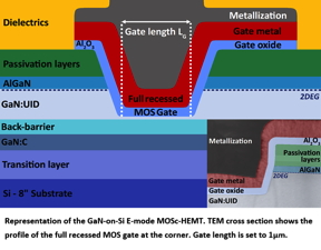
Grenoble, France | Posted on December 17th, 2020In papers presented at IEDM 2020, scientists recounted experiments with variations of high-electron- mobility transistors (HEMT) based on gallium nitride-on-silicon (GaN-on-Si), called GaN-on-Si HEMT. GaN-based semiconductors improve both performance and reliability of increasingly compact power converters compared to silicon, and AIGaN/GaN HEMTs have shown potential to replace power-conversion solutions based on Si or SiC for high-frequency applications with high power and low noise. This technology is therefore expected to be a cost-effective, power-conversion solution for many end-user applications, ranging from smartphones to kitchen appliances and e-vehicles and from battery loaders to DC/DC or AC/DC converters.
Considered together, the two papers provide a novel understanding of the gate stack of the GaN MOS-c HEMT developed at CEA-Leti in the IRT Nanoelec framework. They demonstrate the complexity of GaN MOS stack characterization as well as the requirement for deep expertise to report and analyze reliable parameter values. The work presented in these papers will also help to solve detrimental effects occurring in GaN devices to improve reliability, which is one of CEA-Leti’s key missions during an industrial transfer.
“Carbon-Related pBTI Degradation Mechanisms in GaN-on-Si E-Mode MOSc-HEMT”
This paper investigated the physics behind positive-Bias Temperature Instability (pBTI) effects that occur when transistor gates are positively biased, to determine the root cause of this effect and to minimize it.
“We showed that the instabilities of voltage threshold (Vth) under positive gate stress were caused by two populations of traps,” said Aby-Gaël Viey, an author of the paper. “The first is related to defects in the gate oxide, which is a known effect, and the second to the presence of carbon atoms in nitrogen sites in GaN at the gate interface, which was a discovery, thus confirming the conclusions presented at IEDM.”
Generally in MOS technology where BTI is a common reliability test, e.g. Si/SiGe/Ge-based CMOS technologies, the root causes of Vth instabilities are related to oxide defects that can be charged or discharged by electrons or holes depending on device type (n/p-MOS) and bias polarity. In the case of GaN MOS-c HEMTs, the epitaxial structure grown underneath the transistor is extremely complex and far from homogeneous.
This study also confirmed the conclusions of the work CEA-Leti reported in an IEDM 2019 paper that showed that carbon in GaN-in-N [CN], which usually is introduced as a deep acceptor to create a semi-insulating GaN layer for breakdown-voltage management, is responsible for a part of the BTI instabilities along with the common oxide traps charging. The epitaxial structure is thus a great concern to reduce and minimize instabilities in GaN power devices.
“In addition, our more recent work demonstrated that it is possible to accurately model and predict these threshold voltage instabilities with great precision,” Viey added. “Indeed, the known model of capture emission time (CET) maps were used to confirm the presence of the two populations of traps and predict pBTI degradation (Vth shift) under a certain gate/temperature stress condition.”
“A Novel Insight on Interface Traps Density (Dit) Extraction in GaN-on-Si MOS-c HEMT”
This study set out to characterize the oxide/GaN interface electrical quality to understand if the interface trap density of CEA-Leti’s gate stack was the main threshold voltage (Vth) contributor in GaN-on-Si MOS-c HEMT, and to confirm the performance of the institute’s solution developed during 10 years of R&D.
Dit extraction extracts the density of interface defects that are electrically active at an oxide/semiconductor interface, as well as its distribution in terms of energy with the bandgap of the semiconductor. It is important because Vth is directly related to physical parameters such as metal-gate work function and doping of the semiconductor, which are easily adjustable, and to some defect-related parameters such as fixed or mobile charges in the oxide and interface state density. This density can dramatically influence Vth if the interface is not correctly passivated and processed.
In the case of GaN MOS-c HEMTs, the GaN is dry-etched before oxide deposition and this aggressive process step can have a tremendous impact on the future oxide/GaN interface. Thus, having an accurate and reliable characterization technique of this interface is a requirement to develop and optimize MOS-based GaN power devices. “For other industries or researchers, this kind of approach would help to assess the interface trap density,” said William Vandendaele, an author of the paper.
Vandendaele said the next steps for CEA-Leti researchers are to expand the teams’ understanding of gate-stack optimization of GaN MOSc HEMTs to minimize Dit values, and to transfer the best product, process and characterization methodology to the institute’s industrial partners in IRT PowerGan.
CEA-Leti will pursue its GaN roadmap with further research on epitaxy, devices, passive components, co-integration, and system architectures to develop a GaN technology that allows switching frequencies in the MHz and power densities 10 times those of silicon — all using standard CMOS processes to keep costs down.
Part of this work has been achieved in the frame of IRT Nanoelec.
####
About CEA Leti
Leti, a technology research institute at CEA, is a global leader in miniaturization technologies enabling smart, energy-efficient and secure solutions for industry. Founded in 1967, CEA-Leti pioneers micro-& nanotechnologies, tailoring differentiating applicative solutions for global companies, SMEs and startups. CEA-Leti tackles critical challenges in healthcare, energy and digital migration. From sensors to data processing and computing solutions, CEA-Leti’s multidisciplinary teams deliver solid expertise, leveraging world-class pre-industrialization facilities. With a staff of more than 1,900, a portfolio of 3,100 patents, 10,000 sq. meters of cleanroom space and a clear IP policy, the institute is based in Grenoble, France, and has offices in Silicon Valley and Tokyo. CEA-Leti has launched 65 startups and is a
member of the Carnot Institutes network. Follow us on www.leti-cea.com and @CEA_Leti.
Technological expertise
CEA has a key role in transferring scientific knowledge and innovation from research to industry. This high-level technological research is carried out in particular in electronic and integrated systems, from microscale to nanoscale. It has a wide range of industrial applications in the fields of transport, health, safety and telecommunications, contributing to the creation of high-quality and competitive products.
For more information: www.cea.fr/english
For more information, please click here
Contacts:
Press Contact
Agency
+33 6 74 93 23 47
Copyright © CEA Leti
If you have a comment, please Contact us.Issuers of news releases, not 7th Wave, Inc. or Nanotechnology Now, are solely responsible for the accuracy of the content.
Bookmark:


| Related News Press |
News and information
![]() Simulating magnetization in a Heisenberg quantum spin chain April 5th, 2024
Simulating magnetization in a Heisenberg quantum spin chain April 5th, 2024
![]() NRL charters Navy’s quantum inertial navigation path to reduce drift April 5th, 2024
NRL charters Navy’s quantum inertial navigation path to reduce drift April 5th, 2024
![]() Discovery points path to flash-like memory for storing qubits: Rice find could hasten development of nonvolatile quantum memory April 5th, 2024
Discovery points path to flash-like memory for storing qubits: Rice find could hasten development of nonvolatile quantum memory April 5th, 2024
Possible Futures
![]() Discovery points path to flash-like memory for storing qubits: Rice find could hasten development of nonvolatile quantum memory April 5th, 2024
Discovery points path to flash-like memory for storing qubits: Rice find could hasten development of nonvolatile quantum memory April 5th, 2024
![]() With VECSELs towards the quantum internet Fraunhofer: IAF achieves record output power with VECSEL for quantum frequency converters April 5th, 2024
With VECSELs towards the quantum internet Fraunhofer: IAF achieves record output power with VECSEL for quantum frequency converters April 5th, 2024
Chip Technology
![]() Discovery points path to flash-like memory for storing qubits: Rice find could hasten development of nonvolatile quantum memory April 5th, 2024
Discovery points path to flash-like memory for storing qubits: Rice find could hasten development of nonvolatile quantum memory April 5th, 2024
![]() Utilizing palladium for addressing contact issues of buried oxide thin film transistors April 5th, 2024
Utilizing palladium for addressing contact issues of buried oxide thin film transistors April 5th, 2024
![]() HKUST researchers develop new integration technique for efficient coupling of III-V and silicon February 16th, 2024
HKUST researchers develop new integration technique for efficient coupling of III-V and silicon February 16th, 2024
Nanoelectronics
![]() Interdisciplinary: Rice team tackles the future of semiconductors Multiferroics could be the key to ultralow-energy computing October 6th, 2023
Interdisciplinary: Rice team tackles the future of semiconductors Multiferroics could be the key to ultralow-energy computing October 6th, 2023
![]() Key element for a scalable quantum computer: Physicists from Forschungszentrum Jülich and RWTH Aachen University demonstrate electron transport on a quantum chip September 23rd, 2022
Key element for a scalable quantum computer: Physicists from Forschungszentrum Jülich and RWTH Aachen University demonstrate electron transport on a quantum chip September 23rd, 2022
![]() Reduced power consumption in semiconductor devices September 23rd, 2022
Reduced power consumption in semiconductor devices September 23rd, 2022
![]() Atomic level deposition to extend Moore’s law and beyond July 15th, 2022
Atomic level deposition to extend Moore’s law and beyond July 15th, 2022
Announcements
![]() NRL charters Navy’s quantum inertial navigation path to reduce drift April 5th, 2024
NRL charters Navy’s quantum inertial navigation path to reduce drift April 5th, 2024
![]() Discovery points path to flash-like memory for storing qubits: Rice find could hasten development of nonvolatile quantum memory April 5th, 2024
Discovery points path to flash-like memory for storing qubits: Rice find could hasten development of nonvolatile quantum memory April 5th, 2024
Interviews/Book Reviews/Essays/Reports/Podcasts/Journals/White papers/Posters
![]() Simulating magnetization in a Heisenberg quantum spin chain April 5th, 2024
Simulating magnetization in a Heisenberg quantum spin chain April 5th, 2024
![]() Discovery points path to flash-like memory for storing qubits: Rice find could hasten development of nonvolatile quantum memory April 5th, 2024
Discovery points path to flash-like memory for storing qubits: Rice find could hasten development of nonvolatile quantum memory April 5th, 2024
Industrial
![]() Boron nitride nanotube fibers get real: Rice lab creates first heat-tolerant, stable fibers from wet-spinning process June 24th, 2022
Boron nitride nanotube fibers get real: Rice lab creates first heat-tolerant, stable fibers from wet-spinning process June 24th, 2022
![]() Nanotubes: a promising solution for advanced rubber cables with 60% less conductive filler June 1st, 2022
Nanotubes: a promising solution for advanced rubber cables with 60% less conductive filler June 1st, 2022
![]() Protective equipment with graphene nanotubes meets the strictest ESD safety standards March 25th, 2022
Protective equipment with graphene nanotubes meets the strictest ESD safety standards March 25th, 2022
![]() OCSiAl receives the green light for Luxembourg graphene nanotube facility project to power the next generation of electric vehicles in Europe March 4th, 2022
OCSiAl receives the green light for Luxembourg graphene nanotube facility project to power the next generation of electric vehicles in Europe March 4th, 2022
|
|
||
|
|
||
| The latest news from around the world, FREE | ||
|
|
||
|
|
||
| Premium Products | ||
|
|
||
|
Only the news you want to read!
Learn More |
||
|
|
||
|
Full-service, expert consulting
Learn More |
||
|
|
||