|
In this issue NanoNews-Now Editor Rocky Rawstern covers Memory and Chip Technology in an interview with Greg Schmergel, President and CEO of Nantero, Inc.
Michael E. Thomas, CEO/President/Chairman of Colossal Storage Corporation, contributes New nanotechnology to solve future digital data storage problems.
Off the main topic: in the next in a monthly series, contributing writer Pearl Chin contributes an article titled Is the Nanotechnology Index (NNZ) just a bunch of bull?.
Join us as we present "Memory and Chip Technology - Down We Go"
|
Would knowing the status of patents and patents pending coming out of universities benefit your company? Would having a single database within which to learn how to contact the right person at each technology transfer office be useful?
Nanotechnology Now is pleased to announce our NanoTech-Transfer monthly report and database.
The NanoTech-Transfer product is an excellent tool, as it provides up to date information on what institutions and what individuals are actively involved in filing nanotechnology intellectual property. It provides me with the information I need to stay in touch with the leaders in the field. Great product.
—Douglas W. Jamison, Vice President Harris & Harris Group Inc. hhgp.com
A year's subscription includes 12 issues of our monthly report published on the last Friday of the month, and access to our patent database.
NanoTech-Transfer Patent Database
Full search Database - search by tech-sector, inventor, institution, application, patent number or date.
NanoTech-Transfer Report
Each monthly issue of the NanoTech Transfer Report delivers detailed information on the latest nanotech patents and patents pending from individuals, universities and research institutes from around the world.
Click Here For Details
|
|
Table of contents:
Greg Schmergel
Michael Thomas
Pearl Chin
Quotes
Next Issue
Glossary
NanoStrategies
NanoTech-Transfer
NanoNews Digest
About Us
Contact
|
NanoNews-Now
Editorial Calendar |
|
Aug '04 |
Jobs |
|
Sep '04 |
Life Extension |
|
Oct '04 |
Space Elevator |
|
Nov '04 |
Investments |
|
Dec '04 |
Self Assembly |
|
Jan '05 |
Patents |
|
Return to Top

|
Interview with
Greg Schmergel
Co-founder, President & CEO of Nantero
|

|
Questions by Rocky Rawstern
What is your definition of nanotechnology?
We subscribe to the definition of nanotechnology developed by the US National Nanotechnology Initiative. (Click here for details.)
It is more restrictive than most definitions, but contains critical distinctions that help guide people to true applications of nanotechnology, such as the specification that there must be novel features due specifically to the smaller size.
Do you consider any of your technologies to be nanotechnology?
All of our technologies qualify as nanotechnology under even the most restrictive definitions thereof. We use carbon nanotubes as a key material, and the diameter of a single-walled carbon nanotube is approximately a nanometer. Our memory, NRAM, is nonvolatile because of van der Waals forces which keep the nanotubes permanently in position. And of course that nonvolatility is a very valuable new feature for a random access memory, enabling such advances as an instant-on computer.
Projecting into the next five years, what do you see in terms of investment dollars for memory and chip technologies will there be more or less, and which technologies will receive the lion's share of the funding?
The pace of innovation continues to accelerate, so it would not be surprising to see the amount of investment in new memory technologies increase substantially in the next few years. The impact of new memories on the electronics industry in general and on the value received by the end users of just about electronic device is potentially very noticeable, so memory is going to continue to be a focus within the chip market.
Projecting into the next five years, how do you see memory and chip technologies changing, and what new-technology products may we see on the market?
Nantero certainly plans to have NRAM on the market well within that time frame, combining the nonvolatility of flash with the speed of SRAM and the density of DRAM, all in one chip. NRAM, which stands for nanotube random access memory (or nonvolatile random access memory, since it's both), is ultimately intended to be a universal memory, replacing all of the above memory types, and eventually also hard drives. In the short term, Nantero is focused on specific niches within the memory market, such as embedded memory.
Please talk a little about the process of getting a new technology to market. What are some of the hurdles?
One of the biggest hurdles in putting nanotubes into a semiconductor product was developing methods and processes that are completely compatible with existing CMOS tools and processes. To minimize our licensees' capital expenditures, we had to limit ourselves to using existing fab equipment and processes. We also had to convert generic nanotubes into a fab-compatible material, which is a complex process involving many challenges such as the removal of metallic contaminants. Between making nanotubes fab-compatible and developing processes that allow them to be positioned on silicon wafers appropriately, we've broken through the barriers and enabled carbon nanotubes to be productive parts of new chips.
There are many R&D efforts underway that are attempting to use carbon nanotubes in memory and chip applications. What is your opinion regarding possible success stories, and where do you see roadblocks to success?
Using carbon nanotubes in an R&D environment is very different than using them in a production environment, particularly in a production CMOS fab, all of which have extremely rigorous standards. So that means there is a huge gap between creating one device with attractive properties in a research lab and manufacturing millions of devices with acceptable yields in a production fab. Nantero's joint project with LSI Logic is the first one in the world in which nanotubes are being used in a production CMOS fab.
In your opinion, what other non-silicon technologies are looking good for computer memory and processors?
Now that the materials and processes are in place for using carbon nanotubes in a production CMOS fab, carbon nanotubes can finally move beyond the lab stage. Nantero is using them for various applications, such as memory devices, and is working to support other companies which are making other products in a CMOS fab.
|
Co-founder, President & CEO. Greg Schmergel was most recently Senior Vice President, Corporate Strategy for About, Inc., the 5th largest Web property. Previously he was President and CEO of ExpertCentral.com, Inc. Greg founded ExpertCentral in November 1998 to provide consumers and small businesses with access to thousands of experts to use as an online resource for important questions on a wide variety of topics.
Nantero is a nanotechnology company using carbon nanotubes for the development of next-generation semiconductor devices. These devices include memory, logic, and other semiconductor products. In the field of memory, Nantero is developing NRAMô, a high-density nonvolatile Random Access Memory. The company's objective is to deliver a product that will replace all existing forms of memory, such as DRAM, SRAM and flash memory, with NRAMô serving as universal memory. The potential applications for the nonvolatile memory Nantero is developing are extensive and include the ability to enable instant-on computers and to replace the memory in devices such as cell phones, MP3 players, digital cameras, and PDAs, as well as applications in the networking arena. NRAMô can be manufactured for both standalone and embedded memory applications.
|
Return to Top
|
NEW NANOTECHNOLOGY TO SOLVE FUTURE DIGITAL DATA STORAGE PROBLEMS
|

By Michael E. Thomas
CEO/President/Chairman of Colossal Storage Corporation
|
My invention and patents on a technique for changing matter at the molecular level is one of the World's only new enabling technologies, having many hundreds of electro-optic applications, a few of which are discussed in this article.
Atomic Holographic Nanotechnology will allow for the first time a functional method for programmable molecular lenses that will allow incoming light to be rejected, modified internally, or allowed to pass unaltered through a transparent lens known as disk, tape, card, drum, film, etc.
By being able to program optical lenses, many applications based on light and color can be developed, such as holographic storage, bio-terror detection devices, optical electronics, security products, and hundreds of other products never seen before on the world's markets.
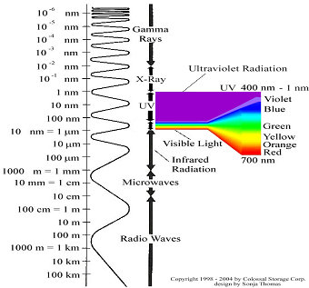
I invented and patented the world's first and only concept for non-contact UV photon induced electric field poling of ferroelectric non-linear photonic bandgap crystals, which offers the possibility of controlling and manipulating light within a UV/Deep Blue frequency of 1 nm to 400 nm.
The small size of ferroelectric transparent structures makes it possible to fabricate nano-optical devices, such as volume holographic storage, having both positive and negative index of refraction that will allow molecular particles of an atomic size to be modified, controlled, and changed to perform a specific function, desired task, used for low cost accurate chemical / biological matter detection, and reprogrammed to accept new non-volatile data and molecular functions.
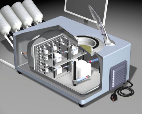
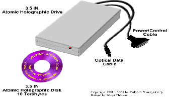
The expected cost of the Atomic Holographic DVR disc drive will be from $570 to $750 with the replacement discs for $45.
One 10 terabyte to 100 terabyte 3.5 in FEdisk would be EQUAL to a 10,000 to 100,000 Gigabyte disk drive.
That's greater 1,000 times any State of the Art hard disk technology with 100 Gigabytes on one disk.
2 EXABYTES of NEW data is generated every year world wide, and growing.
Background of the Storage Industry and the Need for Storage
As the inventor of Atomic Volume Holographic Optical Storage and a 30 year pioneer in the development of peripheral storage technologies, I am the holder of various patents, which Colossal Storage Corporation has licensed.
In 1974 I was making 5 Megabyte disk packs - the biggest at that time in the world. At the same time, IBM, Burroughs, Honeywell, and other Computer professionals said no one would ever need that much storage.
In 1989 Bill Gates (the Chairman of Microsoft) said that the personal computer would never need more than 256 kbytes of cache memory and 40 megabytes of hard drive storage. Today's PC has on average 64 megabytes of cache and 20 to 60 gigabyte hard drives.
As you can see, from a humble beginning data storage has grown considerably in size, and all market data points to its continued growth annually at > 30 %, while some predict data storage doubling every 4 months.
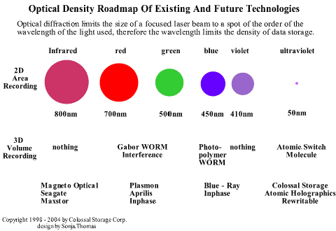
The need for new storage technology is evident to only to those having backgrounds in data storage. The obvious reasons are that the primary source of cheap storage has been the 2D Area hard drives for the last 40 years, IE: 2D Area Technology is technology that only allows the peripheral device to read/write the surface of the disk, tape, card, or drum (x,y).
Present Day Data Storage Technology
Hard drives of today will be reaching their paramagnetic limit - or maximum data storage capacity - in the next few years. Hard drives also write and read data in a serial format, I.E.: they write and read data one bit at a time. The maximum data transfer rate of a hard drive read/write head is approximately 320 megabits/sec. Hard drives are also energy inefficient, and the data storage farms using them were responsible for major power cost overrun problems in the State of California in 2001.
As the Internet continues to grow and more people come to use computers, an integral part of successful growth lies with the peripheral data storage drive.
Some future concerns are being addressed by new DVD, RW/DVD, Blu-Ray etc., but here again we are addressing a 2D Area Storage technology that is in most cases a write-once read-many-times or limited write-read many times RW/DVD.
Here again, due to 2D Area technology, we haven't advanced the bandwidth requirements for future computer users. DVD / Blu-Ray optical technology is a stepping-stone till the Holy Grail of Storage - Rewritable 3D Volume Holographic Optical Storage - starts to come on the market in the next 3 to 5 years.
Data Storage Problems on the Horizon
Data capacities at universities, corporate research facilities, biological research, and data banks are seeing demands continue to challenge the need for faster, bigger, and cheaper storage.
Stanford Linear Accelerator said their storage in first three months of 2002 was 30 terabytes, and predicts at the end of the year their basic research will require >3 petabytes of fast online storage.
Genetics research can take >500 terabytes of storage, according to industry researchers; Oracle the largest data base company predicts data storage to become critical in the years ahead unless new better technology is created.
Future Data Storage Technology
It took me 14 years to find a practical conceptualization that would work to advance the storage industry; 3D Volume Holographic Optical Storage Nanotechnology, for which I hold the patents.
IBM, Lucent, Bell Labs, Philipps, US Government and US Military looked at ferroelectrics, Lithium Niobate and other molecules, but the method of their physics masked the true operation and capabilities of ferroelectrics.
They gave up, saying ferroelectrics couldn't be used. IBM and others used 2 laser photons - one for data and one for reference, the modulation frequency a lot like an AM or FM radio.
The problem they didn't see was they were storing data in the electrons. This makes the ferroelectric data destructive readout (data is destroyed when read), slow and unreliable.
Colossal Storage Theory of Operation of Patented Technology
I gave up two times because I was not able to work thru a concept of non-volatile, non-destructive readout. I finally had a break thru when reviewing Einstein/Plank and Niels Bohr Atomic Theories.
I found that by using an Ultra Violet Photon and an Electric Field it was possible, theoretically, to use the electrons (write current) to make the binary state molecule transition back and forth between the two states. The "Atomic Switch" was born.
The concept of an atomic or molecular switch by "Photon/Laser Induced Electric Field Poling" existed. By using UV photons of lesser quantum energy it was possible to use diffraction and interference from the binary states of the molecule.
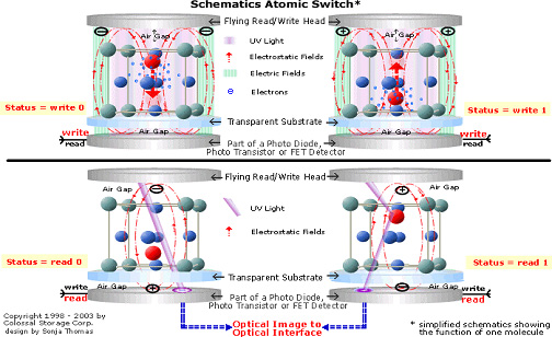
The changing state of the molecule and the diffracted photons allowing for a group of light and dark lines to be characterized as data. 3D Volume means reading and writing
billions of bits at one time in Volume (x,y,z).
Research and Development Unknowns
What is the optimum ferroelectric ceramic crystal molecule for UV/blue laser diode frequency and quantum energy needed to cause electron movement from valence to conduction band?
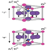
This schematic shows the principle of ferroelectric ram. an ion in the lattice is permanently polarized in either the '0' or '1' position for binary memory.
|
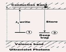
Schematic level diagram of ultraviolet photo refraction effects in ferroelectric.
|
- What is the necessary field strength to cause electron movement in ferroelectric molecule to allow ferroelectric perovskite dipole switching?
- What is the optimum head to media spacing?
- What is the minimum and maximum linear or radial velocity of the media to head?
- What is the optimum read non-destruct laser UV/blue frequency and quantum energy?
- What is the angle of the 2nd read laser UV led?
- What are the light/photon characteristics of diffraction, refraction, luminescence, reflection, etc. from/to the ferroelectric ceramic crystal molecule?
- What are the characteristic of the photo diode and the mosfet read components?
- What is the maximum track densities, 100,000 and higher?
- What are the possibilities for complex encrypted multiple bit storage?
- Is MOCVD the best way to deposit ferroelectric perovskite molecules on a substrate of glass, metal, ceramic, or plastic?
- What type of binder and overcoat is needed?
- What conditions will need to be optimized for spindle motor noise?
- What type of air dynamics for media enclosure, pressures, exotic air mixtures needed?
- What are the maximum allowable temp, shock, humidity ranges?
- What is the maximum signal to noise ratio and is it possible to go further than 200 Terabits sq.in or 40,000 Terabits cu. cm?
- What is the maximum sustained burst data transfer rates?
These and hundreds of other questions come to mind for this new and fascinating atomic holographic optical storage.
This is why Colossal Storage calls the FeDrive the New Frontier, since most of the questions about today's magnetic storage technology were answered many decades ago.
Present day magnetic storage technology is destined to be obsolete due to the paramagnetic boundary limit. Colossal Storage has created a revolutionary concept to keep pace with requirements of mass data storage, for the next millennium.
Advantage of Rewritable Atomic Holographic Optical Disk Drive Storage
Colossal Storage wants its 3D Volume Holographic Optical Storage to be an "all in one" storage solution replacing Ram, Rom, DRAM, Ovonic, Flash, 2D Optical Drives, Tape Drives, and Hard Drives for "all in one" complete system hardware storage requirements.
- New novel storage media - Ferroelectric Molecular Holographic Optical
- New novel integrated semiconductor FE Read/Write Head
- New novel recording using UV/Blue Laser Diode and electric field transducer
- Potential bit density far exceeding present/future drive technology
- Extremely Fast Switch Sub nanosecond State Change
- Extremely High Read and Write Data Transfer Rates
- Extended Temperature Range
- No Altitude Requirements
- Dense Packed Crystallis with densities >200 Tbits/sq.in.
- 8 cents per Gigabyte versus Hard Drives cost of $ 1.00 cents Gigabyte
- 1 10 Terabyte Removable Rewritable Fedisk will be $ 45
- 1 10 Terabyte Fedisk = 20,000 DVD's or 4,000 Blu-Ray
- Download 6,840 raw uncompressed TV Hours
- Initial cost per gigabyte be greater than hard drives to recapture R&D expenses
- No Power Requirements for Media - Non Volatile Media
- Much higher sales margins for media, heads, and drive than data storage
Hundreds of Other Technologies Will Be Enabled By The Atomic Switch
The Photon/Laser Induced Electric Field Poling Theory has many other nanophotonic or nanomolecular uses:
- 3D Holographic Interactive Multimedia Storage Tablet
- Multiple different boot operating systems on common CPU platform Holographic Storage
- 2D/3D Holographic Disk/Card/Drum Storage
- 2D/3D Holographic Disk/Card/Drum VCR
- 2D/3D Holographic Disk/Card/Drum Camera/Photography
- 2D/3D Holographic Xerography and Maskless Lithography Tool
- Programmable UV/deep blue Laser Photon Emitter Source
- 3D Holographic Murals and Window Glass of any size for home, office, museum, skyscraper, and movie theatres
- 3D Holographic programmable camouflage coatings and programmable stealth photonic invisibility screens
- Programmable Holographic nanoSwitch for High Speed Bidirection Optical Transmission & Receiver Telecommunications
- 2D Programmable MEMS nanooptical reflective switches
- 2D/3d Programmable nanomotors, nanoconveyors, nanoneedles, nanopipes for fluid control
- 2D/3D Holographic Programmable nanoWiring
- 2D/3D photonic optical NLO crystal nanotransistor to densities > 40,000 tera-transitors/cu.cm. HP , Intel , and IBM
- Anthrax and other molecules bioparticle detection and classification
- Ferroelectrically Nanocontrolled Biological Particle/Molecule
- 2D/3D Holographic nanoIntegrated Circuit Photolithography for rewritable in circuit reformation fabrication of existing nanocircuits
- 2D/3D Photonic/Molecular/Atomic nanoSwitches for Broadband Telecommunications
- 2D/3D nanoLight Valves and nanoRelays
- Precision Reprogrammable Holographic nanoLenses
- Programmable Holographic Color Filters for UV light, etc.
- Holographic Storage for the Film Industry and other Copyrighted sources for Absolute Protection from IT Theft
- Quantum Molecular Computing
|
Michael E. Thomas, CEO/President/Chairman of Colossal Storage Corporation. The inventor of rewritable ferroelectric molecular optical storage nanotechnology, Michael is a 30 year pioneer in the development of many data storage technologies. He saw NanoTechnology as a new frontier in biological science, electronics, medicine, military, space, transportation, telecommunications, physics, chemistry, and hundreds of other sciences and business. He then patented a unique nanoprocess that would be the next industrial revolution and used his background in storage to facilitate the advancement of his NanoTechnology concepts, the theory of UV photon induced electric field poling of ferroelectric binary dipole dielectric NLO optical molecules. 3D Volume Holographic Optical Storage NanoTechnology is now under research and development.

|
Is the Nanotechnology Index (NNZ) just a bunch of bull? |
 |
In April 2004, Merrill Lynch launched the Nanotechnology Index (NNZ) to be quoted intraday by the American Stock Exchange. First Trust also launched a Nanotechnology mutual fund, FTNATX, this past March 2004. There is already a Munich and Luxembourg based Nanotech mutual fund launched Nov. 2002 and Sept. 2003, respectively. However with the advent of Merrill Lynch into the fray, it validates Nanotechnology in the investment community. So the investment companies are finally hopping on the nanotech bandwagon.
In their Technology Strategy updates on nanotechnology, Merrill Lynch says the criteria by which they choose companies to be on the NNZ index is that the companies must indicate in public documents that nanotechnology initiatives represent a significant portion of their future activities. There are currently 24 companies in their index but they admit they will rebalance the list quarterly. It is unfortunate that giants such as IBM, DuPont and HP who do a significant amount of nanotech research are not included using those qualifications. In addition, Flamel, listed on the NNZ, is not the only publicly traded bio-nano company just like Veeco on the NNZ list is not the only publicly traded instrumentation company that supplies the nanotech research community.
However, there are many nanotech companies that don't want to classify themselves as nanotech so as to maintain their competitive advantage. In business, there is usually not a good reason to publicly disclose your strategic activities to your competitors. Some companies also don't need to if they've always been doing it.
Merrill Lynch is right about nanotech being an approach, a concept which I champion and introduced to them. What nanotechnology is really about, is a better approach to what we've been doing all along but now we can see and manipulate even smaller things. It is akin to when Anton Van Leeuwenhoek invented the microscope. This opened up a whole realm of being able to understand nature better by being able to observe cells and bacteria and blood capillaries that could not be seen before. This ability to much better see small things allowed new scientific breakthroughs in biology and medicine.
When science discovered the electron, it paved the way for new technical breakthroughs in electronics which affects just about everything. The term microtechnology or microelectronics conjures up images of integrated circuit chips which affects many industries also. Nanotechnology is the same. The term nanotechnology makes those who understand microtechnology more comfortable but the label is no less illuminating. However, it is understandable that for most people, they feel more comfortable having a label whether or not it really means something.
Ideally, there can not really be a nanotechnology index or nanotechnology mutual funds because nanotechnology affects many industries and markets. Similar reasoning as to why there should not be an e-Commerce or Dot.com Index. If they really want a nanotechnology index, its impact would ultimately be reflected by the overall manufacturing indices. That being the case, there's no need for a nanotechnology index if there's already a similar indicator, even though it's not born of the investment community. Was there a microtechnology index? There is a similar argument against nanotech mutual funds as with nanotech indices.
Merrill Lynch talks about the nanotechnology sector being narrow and full of pure plays. This is correct. However, this is different from saying they are nanotechnology pure plays. I have often been asked what companies are nanotechnology pure plays. There is no such thing as a nanotechnology pure play.
Right now, people are classifying nanotechnology as a subset of other sector activities. A more accurate classification is to have sectors classified under nanotechnology, such as the nanotech side of biotech, which some call Wet Nano or Bio-nano. For the more well-informed and astute, the whole nanotechnology umbrella will soon disappear altogether because the classification is meaningless.
The companies in the NNZ are uncorrelated due to the fact it is full of pure play companies, which explains their stock behavior. Then how useful is the NNZ as an indication of the nanotechnology investment environment?
For the investment firms doing all this, the real money is not in nanotech mutual funds or stocks. So why are they doing this? Marketing.
I am preaching to the choir, but the value being pursued here for an investment firm is to be perceived to be a knowledgeable and credible player in an emerging trend, such as nanotechnology, by producing something that appears as if it is bringing value to the investment community. It tries to accomplish this by educating the investment community through a nanotechnology index and tech strategy reports. I suppose to some extent, an educated consumer is your best customer. However, the purpose for this education is to attract business, similar to using supposedly objective analyst reports, to its real money-making activities in underwriting IPO's and M&A's.
By the way, Merrill Lynch is one of the investment banking firms underwriting the Nanosys IPO. However, Merrill Lynch's venture arm still has yet to invest in nanotechnology startups.
The NNZ gets Merrill Lynch an 'A' for effort and timing but there's plenty of room for improvement. In the end, after getting past the hype, what does it matter if you call it nanotechnology as long as it works and makes money.
Stay tuned for next month's article.
|
Dr. Pearl Chin has an MBA from Cornell, a Ph.D. in Materials Science and Engineering from University of Delaware's Center for Composite Materials and B.E. in Chemical Engineering from The Cooper Union.
Dr. Chin specializes in advising on nanotechnology investment opportunities. She is Founder and Managing General Partner of Seraphima Ventures, focusing on investing in nanotechnology. She is also CEO of Red Seraphim Consulting where she advises investment firms and startup firms on the business strategy of nanotechnology investments. She was Managing Director of the US offices and co-Managing Director of the London offices of Cientifica. Prior to that, she was a Management Consultant with Pittiglio Rabin Todd & McGrath (PRTM)'s Chemicals, Engineered Materials and Packaged Goods group.
Dr. Chin will be advising the Cornell University JGSM's student run VC fund, Big Red Venture Fund (BRVF), on investing in nanotechnology.
She is a Senior Associate of The Foresight Institute in the US and was the US Representative of the Institute of Nanotechnology in the UK. She was an alternate finalist for a Congressional Fellowship with the Materials Research Society.
She was also a Guest Scientist collaborating with the National Institute of Standards & Technology (NIST) Polymer Division's Electronic Materials Group under the US Department of Commerce.
Dr. Chin is a US Citizen born and raised in New York City.
|
Return to Top
Quotes
In a departure from previous reports, I decided to present portions of relevant articles that have made headline over the past year. By the end of these "bits and pieces" you will likely come to the same overall conclusion I did: there is a lot brewing in memory and chip R&D, and we're in for significant change. I continue to be greatly impressed at the shear variety of innovations that may pave the way for faster, cheaper, smaller memory devices and chips. Can ubiquitous computing be that far in our collective future? I don't think so.
Onto to the Quotes:
Gordon Moore made his famous observation in 1965, just four years after the first planar integrated circuit was discovered. The press called it "Moore's Law" and the name has stuck. In his original paper, Moore observed an exponential growth in the number of transistors per integrated circuit and predicted that this trend would continue. Through Intel's relentless technology advances, Moore's Law, the doubling of transistors every couple of years, has been maintained, and still holds true today. Intel expects that it will continue at least through the end of this decade.
Link
Armed with new investment, Nanochip Inc. (News, Web) expects to make a memorable impact on the removable storage market.
The Oakland, Calif., firm today received $20 million from a syndicate of institutional and industry investors, including Microsoft Corp. (Nasdaq: MSFT, News, Web). That is about $5 million more than the company sought during its second funding round. "I think the reason we got so much is that a lot of people wanted to invest. It definitely exceeded our expectations," Gordon Knight, Nanochip's chief executive Link
Millipede is based on two "breakthrough technologies," according to IBM: thermomechanical recording, in which an extremely sharp tip on a microcantilever with an integrated heater makes and reads back nanometer-scale indentations in a specialized polymer film; secondly, creation and integration of thousands of thermomechanical probes in a micromechanical array, married with a micromechanical actuator that scans the probes over the polymer surface to store and retrieve data in various locations on the film.
IBM plans to target flash memory immediately, a potential $10 billion market. Beyond that, Millipede could have implications in biotechnology and other nanotechnology fields.
"Millipede will likely offer a cost per gigabyte approximately five times cheaper than flash in high-end cards," Andrews says. "Millipede would make a lot of sense in devices like PDAs and smart phones."
Christopher Andrews, IBM Communications Program Manager
Link
The goal of the nano "guitar" and other tiny "instruments" isn't to make music, but rather to use very small devices that vibrate at very high frequencies to find ways to create cheaper electronics that save energy. "One of our major advances has been to learn how to use light beams to cause things to vibrate," says Craighead. "This is an alternative to using lots and lots of little wires to interact with things. We can use light beams that scan over the surface and start things in motion and detect what goes on. We're trying to figure out what sort of new possibilities are allowed by this optical method of interacting with mechanical devices."
Harold Craighead, professor of applied and engineering physics and co-director of the Nanobiotechnology Center at Cornell University.
Link
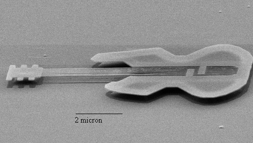
World's Smallest Guitar. Image: CCMR/CNF, Cornell University
The ability to make tiny things vibrate at very high frequencies offers many potential applications in electronics. From guitar strings on down, the frequency at which an object vibrates depends on its mass and dimensions. Nanoscale objects can be made to vibrate at radio frequencies (up to hundreds of megaHertz) and so can substitute for other components in electronic circuits. Cell phones and other wireless devices, for example, usually use the oscillations of a quartz crystal to generate the carrier wave on which they transmit or to tune in an incoming signal. A tiny vibrating nanorod might do the same job in vastly less space, while drawing only milliwatts of power.
Link
|
Contrary to previous understanding, self-replication is unnecessary for building an efficient and effective molecular manufacturing system. Instead of building lots of tiny, complex, free-floating robots to manufacture products, it will be more practical to use simple robot arms inside desktop-size factories. A robot arm removed from such a factory would be as inert as a light bulb pulled from its socket. The factory as a whole would be no more mobile than a desktop printer and would require a supply of purified raw materials to build anything.
"An obsession with obsolete science-fiction images of swarms of replicating nanobugs has diverted attention from the real issues raised by the coming revolution in molecular nanotechnologies," said Drexler. "We need to focus on the issues that matter - how to deal with these powerful new capabilities in a competitive world."
Mike Treder, Executive Director of CRN, said, "We hope that this article will advance the discussion of the actual implications of molecular manufacturing. There is no need for panic, but there are urgent concerns that must be addressed before the technology arrives."
Leading nanotech experts put 'grey goo' in perspective
|
IMEC, Europe's largest independent microelectronics and nanotechnology research center, announces that they have successfully demonstrated the use of high-k dielectrics and metal gates to values below one nanometer. Achieving this level of electrical performance using materials other than the traditional polysilicon-based counterparts removes one of the industry's so-called 'red brick wall' barriers to advancing semiconductor technology.
IMEC breakthrough in high-k/metal gate stacks removes barriers to sub-1nm EOT semiconductor technology development
Link
A group led by Jeffrey Bokor and Yu-Chih Tseng from the electrical engineering department at the University of California, Berkeley, and Hongjie Dai and Ali Javey from Stanford University's chemistry department has made the first working circuit that incorporates both carbon nanotubes and standard silicon technology. Bokor says combining ubiquitous silicon circuitry with the nascent technology to create hybrid electronics will make it easier to introduce carbon nanotube products into the market.
As a proof of principle, the researchers designed the circuit so that the conductivity of each of its 2,000 nanotubes can be assessed individually. This strategy allows the researchers to determine whether a particular nanotube has metallic or semiconducting properties, because CVD tends to give mixtures of the two types of tube. Carbon nanotube makers can therefore use the circuit as a practical tool for determining the ratio of metallic to semiconducting nanotubes from a CVD preparation.
Advancing toward finer circuitry
Link
Researchers say the development brings them a significant step closer to using carbon nanotubes for memory chips that can hold orders of magnitude more data than current silicon chips - 10,000 times greater, according to some estimates - or for sensors sensitive enough to detect traces of explosives or biochemical agents at the molecular level.
"We first envisioned a patterned growth of carbon nanotubes on silicon wafers five years ago, but it wasn't clear at that time whether that approach would work as an integrated nanotube-silicon hybrid circuit," said Dai. "It was the combined expertise in chemistry, materials science and electrical engineering that made this a reality."
Researchers announce breakthrough in nanoelectronics, develop first integrated silicon circuit with nanotube transistors
Link
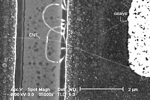
Magnified view of carbon nanotube grown on silicon MOS circuitry. The bright area on the upper right-hand side is the catalyst island upon which the nanotube was grown. (Image courtesy Ali Javey)
|
|
The industries that nanotechnology will likely have a disruptive effect on in the near term include the following:
(Amounts are Billions of US Dollars)
|
$1,700 |
Healthcare |
|
$600 |
Long Term Care |
|
$550 |
Electronics |
|
$550 |
Telecom |
|
$480 |
Packaging |
|
$450 |
U.S. Chemical |
|
$460 |
Plastics |
|
$182 |
Apparel |
|
$180 |
Pharmaceutical |
|
$165 |
Tobacco |
|
$100 |
Semiconductor |
|
$92 |
Hospitality / Restaurant |
|
$90 |
US Insurance |
|
$83 |
Printing |
|
$80 |
Corrosion Removal |
|
$57 |
US Steel |
|
$43 |
Newspaper |
|
$42 |
Diet Supplement |
|
$40 |
Diet |
|
$32 |
Publishing |
|
$30 |
Catalysts |
|
$27 |
Glass |
|
$24 |
Advertising |
|
$18 |
Cosmetics |
|
$13 |
Chocolate |
|
$10 |
Battery |
|
$5 |
Blue Jeans |
|
$4 |
Khakis |
|
$2.8 |
Fluorescent Tagging |
|

The Mother of All Minds
Dudley Lynch


Our Review
The Superswarm Interview
The Superswarm Option
Nanoveau - This column will cover the science, the speculation, and (occasionally) the politics of nanotechnology and related topics. If you want to know what nanotech is about, and how and why it will change everything we know-Nanoveau is for you.
|
|
Tiny tubes of DNA have been developed that could be used to wire nanoscale electronics. To construct the nanotubes, Thomas LaBean and colleagues from Duke University in North Carolina used rigid tiles formed from multiple strands of synthetic DNA. The tubes could be a breakthrough for the self-assembly of nanoscale circuits because they can be targeted to connect at specific locations on large-scale structures and be metallized to form nanoscale wires.
Programmable, self-assembling DNA nanostructures could allow for the positioning of components for molecule electronics.
Link
Super-fast computing and communications devices, among other things, could be the eventual result of a light-emitting transistor developed by University of Illinois researchers. UI Professor Nick Holonyak said the work is at an early stage and it could take decades for the technology to play out. But Holonyak painted a picture of a world in which computing and communications eventually move, in essence, at the speed of light, opening up a myriad of possibilities. "Time and distances ... they become compressed," he said. "You could have access to anything, anywhere in terms of information." He used the example of a doctor consulting with experts around the world during an operation, who see and make suggestions as clearly as if they were in the operating room.
UI 'sitting on a breakthrough'
Link
Computers that boot up almost instantaneously. Cellphones with enough battery-conserving memory to run full-motion video and music files for days. A trillion bits worth of data storage on a chip the size of a postage stamp.
Those are some of the potentially radical implications of technology being developed here by Nantero Corp. Late this year Nantero hopes to start selling computer memory chips built with carbon nanotubes, an ultra-tiny form of matter that is 20 times as strong as steel and conducts electricity 1,000 times better than copper. Nantero claims a potential $100 billion market opportunity.
Link
Carbon nanotube memories could sharply improve the performance of cell phones, laptop computers and other electronic devices. Like today's flash and SRAM memories, carbon nanotube designs can maintain data when power is turned off, an advantage over dynamic random access memory, or DRAM, memory chips, which must constantly be refreshed. But it can operate considerably faster and on less power than flash memory, and is much cheaper and more compact than SRAM.
Link
With today's chipmaking technologies likely to reach physical limits in the next decade or so, researchers have been working on alternative approaches to making smaller computer circuits. One promising possibility is arrays of nanowires whose junctions form tiny, densely packed transistors. Transistors are electrical switches that are the building blocks of computer chips. Nanowires measuring a few nanometers in diameter could enable computer chips that pack a trillion transistors per square centimeter, which is several orders of magnitude more than current chipmaking technologies are likely to achieve.
Link
A team of researchers at Rochester Institute of Technology has developed the ability to use optical microlithography to produce semiconductor device geometry as small as 38 nanometers. The team, led by Bruce Smith, Intel Professor of Microelectronic Engineering and associate dean of the Kate Gleason College of Engineering, used a prototype liquid immersion nanolithography tool developed at RIT.
Smith says microelectronic devices that previously required extreme ultraviolet or near X-ray wavelengths can now be produced with optics and light much closer to the ultraviolet. This allows for more rapid and cost-effective development of smaller, more powerful and more affordable microelectronic devices.
Link
Intel Corp. expects its microprocessors to hit one-billion transistors by 2007, up from 42 million in the current Pentium 4, said Gerry Marcyk, director of components research at Intel's development facility.
While process technology generally moves forward in two-year cycles - with shifts to 90-nanometer lithography design rules expected in 2003, to 65 nm in 2005, then to 45 nm in 2007 - packaging will have to hustle to keep up the pace, Marcyk said.
Link
New electronic clocks smaller than blood cells soon may find their way into microchips to replace bulkier technologies at a greatly reduced cost.
The microclocks, developed by scientists at the National Institute of Standards and Technology, "could lead to shrinking of components in computers, leading to faster and more powerfulcomputing , as well as cell phones , things like global positioning system units, as well as broadband Internet and wireless connectivity," researcher William Rippard, a NIST physicist in Boulder, Colo., told United Press International.
Link
IBM uses a technique developed at the University of Massachusetts that allows polymers to self-assemble into a honeycomb pattern with holes as small as 20 nanometers. The polymers then are placed as a stencil on silicon dioxide, a material compatible with today's chip-making processes, for growing uniform nanocrystals.
The self-assembled honeycomb shape is one of several patterns (IBM researcher Kathryn) Guarini said they want to create using various self-assembling materials. Different geometries would serve different functions as memory or logic devices. And their self-assembly system could complement other nanotechnology initiatives at IBM, such as efforts to construct transistors using carbon nanotubes.
IBM is in a race with companies such as Intel Corp., Hewlett-Packard Co. and Motorola Inc. to shrink components on chips for smaller, faster computing devices.
Link
... such chips might arrive sooner than later. Leading memory makers such as Samsung, Micron (MU ), Infineon (IFX ) and Hynix in DRAM, and flash heavyweights Samsung, Toshiba, Intel (INTC ), and an AMD (AMD )-Fujitsu joint venture, have been ramping up spending on research and development. In fact, experts think memory is likely to get a heftier chunk than usual of the $20 billion Merrill Lynch expects chipmakers to spend on R&D this year.
Chipmakers are also working to improve DRAM and flash. Micron is developing a method for putting more memory onto a chip by stacking its components rather than arranging them side-by-side, says Mark Durcan, chief technical officer at the largest DRAM maker in the U.S. And Intel is attempting to reengineer insulators that stand guard at flash memory's door to let saved data in and out.
Another promising technology, being developed by players like IBM (IBM ), Motorola (MOT ), and Samsung, is called magnetic RAM (MRAM). Devices with MRAM, which could appear in products like PCs in the next four years, don't need to be turned off. When not in use, they'll simply fall asleep and stop consuming energy, ready to be awakened at the push of a button instead of via a time-consuming boot-up process. MRAM's secret is that it uses magnetic forces rather than an electrical charge to store data.
Intel, Samsung, and others are also working on phase change RAM (P-RAM) -- also called ovonic memory -- which can process data up to 100 times faster than flash, says Intel's Lai, while at the same time retaining it for easy retrieval. The chip also can be written to about 1 trillion times before it needs replacing vs. 1 million times for flash, Lai says. That's because it's made of the same material as a rewritable DVD.
Work is also progressing on more revolutionary advances -- nanocrystal, molecular, and organic memory -- that have been the subjects of experiments for years.
Link
Organic nanoscopic optical materials have for the first time dipped below the critical 1-volt mark with five times greater speed and other leading edge performance characteristics.
Five times greater speed translates to 5 terabits/s or 625 gigabytes, the researchers said, adding that they achieved 10-fold lower power consumption and 10-fold decrease in manufacturing costs compared with industry standard materials based on lithium niobate crystals.
"We knew we had something a few years ago when our material was twice as fast at one-half the normal voltage, but we wanted to wait to make our big announcement until it was obviously worth taking from the research stage to commercialization," said Alvin Kwiram, a chemistry professor and the executive director of the Science & Technology Center on Materials and Devices for Information Technology Research at the University of Washington.
Link
Thomas N. Theis and Paul M. Horn: For decades now, the cost of a finished Si chip has remained roughly constant, while the number of circuits on that chip has risen exponentially and the cost of information processing has plummeted.
Information storage has a similar story, as exemplified by the history of the hard-disk drive. Storing ever more zeros and ones as tiny regions of magnetization on a spinning disk has resulted in performance improvements and production economies that by many measures exceed even those of the transistor revolution.
Progress in magnetic recording should continue for a good 10 years, with areal data storage densities reaching somewhere between 10 and 100 times today's best values. The shrinking of Si transistors will probably continue for at least another 10 years, until the fairly hard physical limit of quantum tunneling is reached at gate lengths somewhere around 10-20 nm.
However, we see no physical or economic reason why those milestones should mark the end of the road for IT. Indeed, much of the excitement (and some unwarranted hype) surrounding nanotechnology is based on the promise of new devices operating at the molecular scale to sense, process, store, and communicate information. That promise is why companies are exploring the physics of electron transport in carbon nanotubes, semiconductor quantum wires, and a variety of organic molecules; it is also why they are fabricating primitive devices and circuits based on those new components.
Link
Sony Corp. and Toshiba Corp. have agreed to expand their cooperation in the semiconductor field and develop technology for chips two generations past today's most advanced devices. They each plan to invest 10 billion ($94.3 million) in the project which is scheduled to run until the end of 2005. The ultimate goal of the project is mass production of 45nm chips.
Link
Self-assembly has become a critical implement in the toolbox of nanotechnologists. Scientists and engineers who explore the nano realm posit that the same types of forces that construct a snowflake--the natural attractions and repulsions that prompt molecules to form intricate patterns--can build useful structures--say, medical implants or components in electronic chips.
Link
Daniel Gamota, manager for new products manufacturing at Motorola Inc., described his company's work with "printed organic electronics." Working with newspaper printers, and a former silkscreen T-shirt printer, Motorola has been able to print materials with embedded nanoparticles, he said.
"If we're successful, we might be able to print paper that changes color based on temperature or mood," he said. "Or we could print big-screen TVs." Gamota described an "organic FET" that's printed with suspended nanoparticles and nano-composite oxides.
Link
Nippon Telegraph and Telephone Corporation has created an electron beam (EB) lithography system that enables the fabrication of extremely small three-dimensional (3D) structures with sizes measured in nanometers. NTT demonstrated the 3D nanopatterning and nanofabrication by exposing a small sphere to the EB to form the world's smallest globe. This highly advanced technique promises to become the technological foundation of nanotechnology, which is expected to give rise to many new industries and new markets.
Key Features
- 3D nanofabrication and nanopatterning down to the 10-nanometer level.
- A drive that rotates a sample around two axes with a high precision.
- A height sensor that enables the EB to be focused on a 3D sample. The focus error is less than 1-2 micronmeters.
- A new beam-positioning system, which detects the outline of a sample using a transmitted-electron signal for accurate placement of patterns.
Link
Hendrik F. Hamann et al. report bit sizes of less than 40 nm across in a magnetic film. This permits storage densities of 400 billion bits (400 Gbit) per square inch, and further increases of more than twofold seem possible. In contrast, the conventional technology was expected to plateau at around 150 Gbit per square inch.
Researchers from the LG Electronics Institute of Technology in Korea have devised a very low-power method of reading bits of information stored in areas of film that measure 50 nanometers, or 20 times narrower than an E. coli bacterium. The method could eventually be used in ultrahigh-density mechanical storage devices for portable systems like notebook computers, personal digital assistants and digital cameras.
Link
Perpendicular storage is an evolutionary technology which can be produced using existing production lines. It can provide storage capacities of up to 1Tb per square inch, which is equivalent to storing 1TB on a single 3.5-inch disk platter and almost 10 times as much as today's standard longitudinal storage systems.
Link
Researchers there (HP) used nanoimprint techniques to create what they described as the world's smallest rewritable non-volatile memory: an 8-by-8 crossbar sandwich with an active molecular layer caught between two layers of electrodes. The device size, if scaled up, would result in a 6.4 Gbit/cm2 bit density.
Link
"Atomic-level lithography is now possible," Theis said during a keynote address at SPIE in San Jose.
Among these structures using this technique include nanomechical data storage and molecular cascade logic devices. At the event, the IBM researcher discussed the development of a next-generation storage device, dubbed the Millipede, which is based on MEMS technology. The Millipede is a tiny structure that could store 114 terabits of data per square inch at a transfer rate of 800-Gbs per second.
Another future device is a molecular cascade logic device, which is a three-input sorter built around carbon oxide molecules. "We've built this at the atomic scale," he said. "This is the ultimate lithography."
Link
"Growing silicon nanowires in a specific location in whatever direction you desire, which we have done, is much more practical for gigascale integration -- putting a billion transistors on a chip -- in the long term," said Solanki (Raj Solanki, Ph.D., professor of electrical engineering professor in OHSU's OGI School of Science & Engineering).
Link
NanoBridge technology uses the atom switching effect of a nanoscale metal bridge, in which an electrically conductive channel is created or annihilated by stretching a metallic bridge controlled by an electrochemical reaction inside a solid electrolyte. With an easy-to-fabricate, highly stable junction structure and a solid electrolyte (Cu2S) with high process immunity, the NanoBridge stabilizes the LSI wiring layer.
As a result, the operating speed of a programmable LSI device, which is indispensable for short-term equipment development, can be increased and the area of the chip reduced, thus improving performance and lowering costs in electronic appliances such as mobile equipment and digital televisions.
About one-thirtieth the size of the SRAM and pass transistor circuit reconfiguration switch used in a conventional programmable LSI device, the NanoBridge switch can be incorporated directly into the wiring layer. It has one-twentieth or less the resistance of the conventional switch.
Link
Imagine a computer with amazing processing power, a 3D display (literally, not figuratively) instant response, able to run every available OS and application at the same time, virtually no power consumption, zero moving parts and complete security - and whose physical component is about the size of a pack of playing cards. It would also hold every music CD and movie DVD you ever owned, or will own, and still leave space for not only your family album, but your brother's, sister's, aunt's and uncle's too.
Link
Scientists at IBM Research have demonstrated a relatively inexpensive way to use heat to make it easier to write magnetic patterns on such media. The technique could make it possible to store more than one terabit per square inch, according to the researchers. That's nearly 27 DVDs worth of information. The technique would also be relatively fastórecording speeds of more than one billion bits per second, or gigahertz, are possible, according to the researchers.
Link
... one way of cramming more data into a fixed lateral region on a data storage device, other than shrinking the cell's size, is to store more than one bit in each memory cell.
A USC/NASA-Ames collaboration has taken a step in the direction of such a chemical memory by producing a memory cell with three different controllable bit states, with a total of 8 (2 raised to the 3rd power) distinct levels. Data density rates as high as 40 Gbits/cm2 are expected.
Link
Researchers from the Chinese Academy of Sciences have taken a step in this direction by synthesizing an organic material, spreading it into a molecule-thick layer, and recording marks as small as 1.1 nanometers in the medium. The 1.1-nanometer marks, spaced 1.5 nanometers apart, would yield a data storage density of more than 10 trillion bits per square centimeter, according to the researchers.
Link
The primary objective of DARPA's Moletronics Program is to deliver a prototype 16 kbit nanocomputer memory by early 2005. This prototype will be integrated on the molecular scale and have dimensions of ~10 µm x 10 µm, which is approximately the footprint of a human cell. As a result, the target device density for the nanomemory is 100 Gbit/cm2. At this level of integration, the prototype will be ten times more dense than the dynamic random access memory (DRAM) that the Si industry projects it will deliver at the end of its roadmap in 2016.
Link
... researchers in Canada have made a nanostructured plastic in which several different optical bits can be superimposed without interfering with each other. Potentially, this material therefore has a very high storage density. The 'grain size' of the memory is about 1 µm, and each grain contains, in effect, up to three different binary memory elements. Such units have 23 = 8 different memory states, as opposed to just the 1's and 0's of magnetic media.
Link
Researchers from Lucent Technologies' Bell Laboratories, Rutgers University and the University of Illinois have found that the orientation of crystalline organic semiconductors plays a big role in organic transistor performance. The researchers have developed a simple lamination manufacturing process for making transistors from the fragile organic material, and the resulting transistors have set a record for carrier mobility in organic transistors.
Link
Xerox Corp. disclosed details of a nearly complete polymer electronic process that could run on inkjet printers during a presentation at the Material Research Society's spring meeting this week in San Francisco. Beng Ong, a Xerox Fellow who has been spearheading the polymer electronics effort, said three different electronic ink processes could create semiconductors, conductors and dielectrics ó the three ingredients needed for integrated circuits ó in a printable process.
Link
Researchers at the University of Southern California and the NASA Ames Research Center have successfully tested a self-assembled molecular memory device they say has the potential of holding 40 Gigabits per square centimeter -- a far greater density than any achieved on silicon. Furthermore, says Chongwu Zhou, an assistant professor in the USC Viterbi School department of electrical engineering, because of the self-assembly feature, such ultra dense memory devices can likely be cheaper than the silicon flash memories now widely used in digital cameras, "memory sticks" and other applications.
Link
Engineers in the US have made the first high-speed transistor from a carbon nanotube. Peter Burke and colleagues at the University of California at Irvine showed that their device - which consists of a single-walled carbon nanotube sandwiched between two gold electrodes - operates at extremely fast microwave frequencies. The result is an important step in the effort to develop nanoelectronic components that could be used to replace silicon in a range of electronic applications.
Link
Clever geometry is the basis of a new material that is said to be ideal for secure data encryption and dense optical information storage. The material consists of a lattice of onionlike spheres in which the particle core and its layers each contain a different dye. The material can hold four or more pieces of information in one spotónot just two as in binary optical data storage. And it opens a door to high-density three-dimensional optical data storage.
Link
Physicists in Germany and the US have made a single-electron transistor that operates using a nanometre-scale vibrating arm. The device was built using a simple two-step process and does not need to be operated at cryogenic temperatures like previous devices of its kind. It could have a wide variety of practical applications and could also be used to study fundamental physics.
Link
Nantero is creating NRAM, a high-density nonvolatile random access memory chip, which it hopes will replace existing forms of memory. Its technology, using cylindrical molecules of carbon known as nanotubes, will be used on a production line in LSI's semiconductor factory in Gresham, Ore.
Carbon nanotube memories could sharply improve the performance of cellphones, laptop computers and other electronic devices. Like today's flash and SRAM memories, carbon nanotube designs can maintain data when power is turned off, an advantage over dynamic random access memory, or DRAM, memory chips, which must constantly be refreshed. But it can operate considerably faster and on less power than flash memory, and is much cheaper and more compact than SRAM.
UCI's Peter Burke has shown for the first time that transistors made from single-walled carbon tubes only a few nanometers wide operate at extremely fast microwave frequencies.
"I estimate that the theoretical speed limit for these nanotube transistors should be terahertz (1,000 GHz), which is about 1,000 times faster than modern computer speeds," Burke said.
Link
And some may make a great deal of money on this high-speed roller coaster ride, as predicted here:
Business Communications Co. (BCC) projects that nanoelectronic memory devices will enter the market this year, and bring in $200 billion by 2013. Logic devices will have a more modest $20 billion market by 2013.
Link
Worldwide sales of DRAM (dynamic random-access memory) and flash memory combined should grow about 40% this year, to $40 billion, according to chip researcher IC Insights in Scottsdale, Ariz.
Link
From Our Molecular Future: How Nanotechnology, Robotics, Genetics, and Artificial Intelligence Will Transform Our World, by Douglas Mulhall:
-
What happens to the monetary system when everyone is able to satisfy his own basic material needs at very low cost?
-
How would we use cash when digital manufacturing makes it impossible to differentiate a counterfeit bill or coin from the real thing?
-
What happens to fiscal policy when digital information, moving at light speed, is the major commodity?
-
How fast will monetary cycles move compared to, say, the ten- or twenty-year cycles of the late twentieth century, when products and patents go out of date in a matter of months instead of years?
-
What happens when we don't have to worry about trade or social services for our basic needs, because most of what we need is provided locally with digital manufacturing, and the biggest trade is in information?
-
How do we control the excesses of the ultrarich, the overabundance of the molecular assembler economy, and the challenge to intellectual property laws created by intelligent, inventive machines?
-
What happens if half of all jobs are made redundant every decade?
-
What happens to the War on Drugs when there's no import, export, or transport of contraband because drugs can be manufactured in a desktop machine using pirated software downloaded from the Internet?
-
What happens to democratic controls when individuals can get as rich as small governments in a year or so?
-
What's the relevance of insurance if many things are replaceable at very low capital cost, but liabilities from software are potentially unlimited?
-
How should organized labor react when molecular assemblers and intelligent robots eliminate most manufacturing jobs?
-
What is the nature of work going to be?
-
What happens to land prices when an individual can build a tropical farm under a bubble in North Dakota, and get there from New York in an hour?
-
What happens when everyone can go everywhere, whenever they want, and work from wherever they want?
Return to Top
IN THE NEXT ISSUE
Issue #14 will cover Jobs. It will land in your mailbox August 2nd, 2004.
Infamous Quotes:
"This 'telephone' has too many shortcomings to be seriously considered as a means of communication. The device is inherently of no value to us." Western Union internal memo, 1876
"Heavier-than-air flying machines are impossible." - Physicist and mathematician Lord Kelvin, President of the British Royal Society, 1895
"Everything that can be invented has been invented." - Charles H. Duell, Director of U.S. Patent Office, 1899
"There is no likelihood man can ever tap the power of the atom." - Robert Milikan, Nobel Laureate in Physics, 1923
"Theoretically, television may be feasible, but I consider it an impossibility-a development which we should waste little time dreaming about." - Lee de Forest, inventor of the cathode ray tube, 1926
"I think there is a world market for maybe five computers." IBM's Thomas Watson, 1943
"Landing and moving around on the moon offer so many serious problems for human beings that it may take science another 200 years to lick them." - Science Digest, August 1948
"Computers in the future may weigh no more than 1.5 tons." Popular Mechanics, 1949
"There is no reason anyone would want a computer in their home." Ken Olsen, Digital Equipment Corp, 1977
And the lesson is? It's a tough game to call.
Need advice? Check out NanoStrategies
© Copyright 1999-2004 7thWave, Inc. All rights reserved. More information on copyright, and disclaimers regarding the content of this newsletter can be found here
|