|
In this issue NanoNews-Now Editor Rocky Rawstern and contributing writer Robert Folaron (Director - Product Development, Zyvex) cover nanotech tools. We also survey businesses making tools for the nascent nanotechnology industry.
Off the main topic: Contributing writer Pearl Chin (in the next in her monthly series) contributes an article on Nanosys: To IPO or Not to IPO? Is That the Question?.
Join us as we present "Tools of the nanoTrade."
|
Nanotechnology Now is pleased to announce our NanoTech-Transfer monthly report and database.
The NanoTech-Transfer product is an excellent tool, as it provides up to date information on what institutions and what individuals are actively involved in filing nanotechnology intellectual property. It provides me with the information I need to stay in touch with the leaders in the field. Great product.
—Douglas W. Jamison, Vice President Harris & Harris Group Inc. hhgp.com
A year's subscription includes 12 issues of our monthly report published on the last Friday of the month, and access to our patent database.
NanoTech-Transfer Patent Database
Full search Database - search by tech-sector, inventor, institution, application, patent number or date.
NanoTech-Transfer Report
Each monthly issue of the NanoTech Transfer Report delivers detailed information on the latest nanotech patents and patents pending from individuals, universities and research institutes from around the world.
Click Here For Details
|
|
Table of contents:
Robert Folaron
Survey
Pearl Chin
Quotes
Useful Links
Next Issue
Glossary
NanoStrategies
NanoTech-Transfer
NanoNews Digest
About Us
Contact
|
NanoNews-Now
Editorial Calendar |
|
Jul '04 |
Memory & Chip Technology |
|
Aug '04 |
Jobs |
|
Sep '04 |
Life Extension |
|
Oct '04 |
Space Elevator |
|
Nov '04 |
Investments |
|
Dec '04 |
Self Assembly |
|
Jan '05 |
Patents |
|
Return to Top
"The Tools Of The Trade"
The Leading Edge Of Nanotechnology
|

Robert Folaron
Director of Product Development, Zyvex Corporation
|
It is well known that the leading edge of any new industry relies on the successful development and deployment of enabling tools. This is true from the California gold rush of 1849, to the infant semiconductor industry of the 1970s, and is once again true with the application of nano-scale technology. While not yet an "industry," applied nanotechnology is alive and in need of enabling tools. Zyvex Corporation in Dallas, Texas, the world's first nanotechnology company, is a leading provider of such enabling nanotechnology tools.
Getting Started
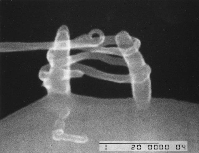
In 1997, Jim Von Ehr founded Zyvex and established a long-term plan to develop atomically precise manufacturing capabilities. We were almost immediately confronted with the reality that no tools existed to perform nanoscale research, at least none that could physically manipulate and assemble nanoscale components. Scanning Electron Microscopes (SEMs) and Transmission Electron Microscopes (TEMs) were great imaging tools to observe nanoscale components, but the specimens could not be physically manipulated in any meaningful way. To remedy this situation, we developed a nanomanipulation tool to further our own nanoscale research of components such as carbon nanotubes. From its inception, the nanomanipulator requirements included an ability to work in high vacuum (10-6 Torr), to deliver two-nanometer precision, and the individual robotic positioners had to be small enough so that at least four of them could work simultaneously in a typical electron microscope chamber. In addition, we required that the system support a future family of robotic end effectors (now called NanoEffectorsô).
After successfully developing and utilizing a second-generation nanomanipulator, we began to understand that we were not alone in our needs, and so we initiated development of a commercial version of our nanomanipulator. At the same time, we updated our business model to support three complimentary business lines to develop and support nanoscale technology: 1) a MATERIALS business line dedicated to the development of advanced materials, 2) a TOOLS business line dedicated to the development of enabling tools for nanoscale research and manufacturing, and 3) a STRUCTURES business line dedicated to the development and proliferation of microscale and nanoscale components and instrumentation.
Delivering the Goods
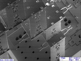
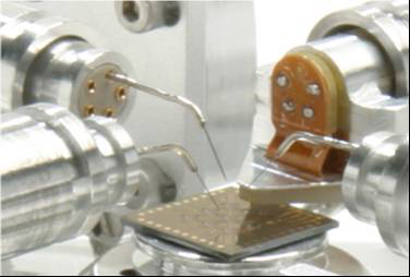
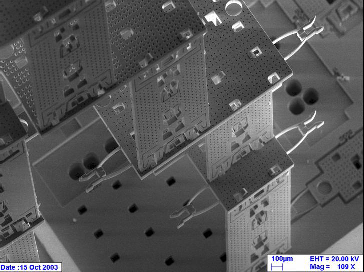
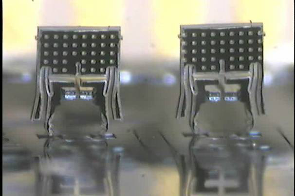
On April 15th, 2003, we introduced the S100 Nanomanipulator for use in SEMs, primarily for the nanotechnology research community in corporations and universities (Figures 1 and 2). Within months, potential customers urged us to develop a nanomanipulator tool that could be used in Focused Ion Beam (FIB) systems, and we then introduced the F100 for use in FEI DB235 Dual Beam FIBs (Figure 17). In the Fall of 2003, we introduced the A100 system for assembly and testing of microscale components. In early 2004, we introduced the L100 system (Fig 19) dedicated to the micro and nano scale R&D activities in the Life Sciences field.
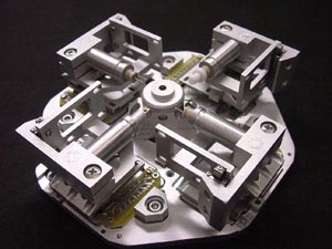
Fig 1: S100 with Four Robotic Positioners
|
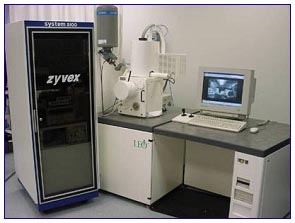
Fig 2: S100 Nanomanipulator system in a LEO SEM
|
Below is a demonstration of how the Zyvex Nanomanipulator provides an interface from the nanoscale world to the macro world of the human interface (Fig 3):
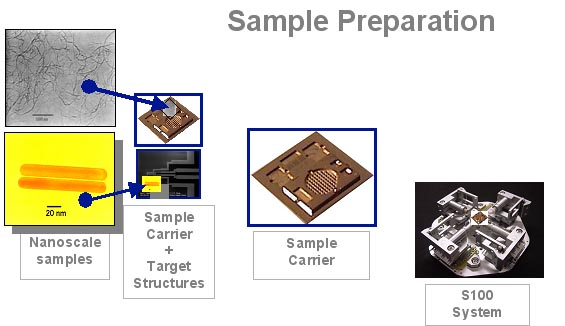
Fig 3: Nanoscale sample preparation for S100 Nanomanipulator
|
End Effectors, Accessories, and Support Tooling
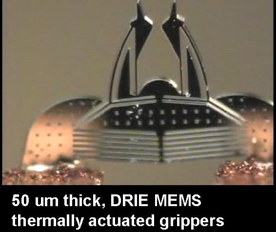
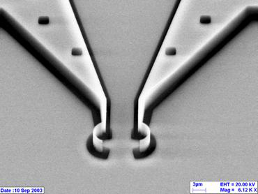
The same market feedback that dictated a need for the S100 system to work in multiple environments also quickly dictated a need to develop a family of robotic end effectors. Subsequently, we introduced (Figures 4-10): 1) Silicon Microgrippers and 2) Probes as useful end effectors on nanomanipulator systems.

Fig 4: 125µm gripper finger opening
Click for large version
|
Fig 5: Simulation of µgripper actuation
Click for large version
|
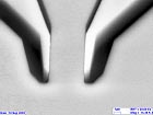
Fig 6: normally open-5µm
|

Fig 7:normally open-10µm
Click for large version
|
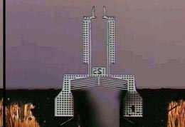
Fig 8: normally open: 125µm
|
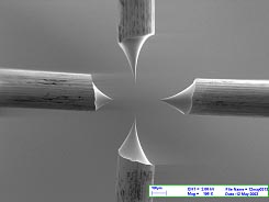
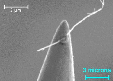
Fig 9: Zyvex probes manipulating CNTs
|
Fig 10: performing device failure analysis
Click for large version
|
Another major product area serving our customers is a product line of "wave drivers." These wave drivers: the mDriver 1000 for testing and characterizing MEMS devices in general, and the tDriver 1600 specifically developed and optimized for thermal MEMS, help MEMS engineers and designers reliably test their MEMS devices. These wave driver systems are sold as fully functional stand alone units for MEMS research and development, as well as fully integrated subsystems within the Zyvex nanomanipulator systems.
We also find that we are continuously developing new robotic positioners for customers, as well as improving existing positioners for new applications. With a stable technology platform from which to work and develop these miniature robots, Zyvex has demonstrated an ability to develop at a pace that ensures timely response to our customers. With recent software architecture advances, the Zyvex family of nanomanipulators now also offers substantial user flexibility and ease of use, as well as 3rd party system integration. All of which means that applied nanotechnology development can now accelerate.
Applications Enabled by Zyvex TOOLS
With a quality nanomanipulator system available to it, the open market quickly moved to use it for a variety of new applications. Below are a few examples of applications enabled by the Zyvex line of micro and nanomanipulator systems.
In 2003, customers were introduced to the ability to manipulate and perform a four-point probe electrical measurement of carbon nanotubes. See figures 11-12 below.
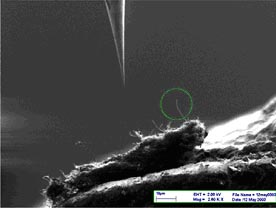
Fig 11: Probe tip approaching carbon nanotube (CNT)
|
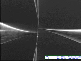
Fig 12: Four-point electrical measurement of CNT
|
Also in 2003, we introduced capabilities to perform precise pick and place with Silicon Microgrippers: Using Microgrippers (µgrippers) with the S100 (figures 13-14 below). Micro grippers can be used for a variety of micro and nano scale operations.
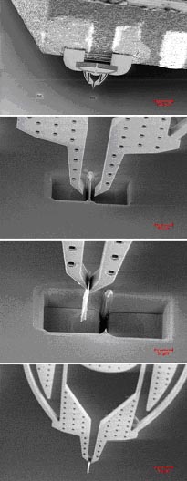
Fig 13: µgrippers pick FIB-cut coupon
|

Fig 14: Standard 5-pin end effector interface
Click for large version
|
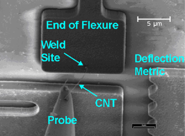
In February 2004, Zyvex introduced an application for: Mechanical Measurement of Individual Carbon Nanotubes Using MEMS and the S100 Nanomanipulator. In this application, the user can extract and measure individual carbon nanotubes with a combination of probes and MEMS flexure components (figures 15-16).
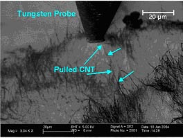
Fig 15: Pulling a single CNT from a sample
|

Fig 16: CNT welded to a probe and a MEMS flexure
Click for larger version. Click here for expanded image of probe and CNT.
|
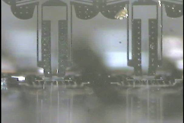
In April 2004, Zyvex introduced an application note specifically targeted to semiconductor manufacturers. As semiconductor devices achieved 90nm, 65nm, and 45nm feature sizes, existing equipment could no longer adequately perform timely failure analysis or yield management of these features. These features are so small that they can only be viewed with an electron microscope. Zyvex's S100 nanomanipulator enables semiconductor manufacturers to probe these features and perform electrical characterization of the various transistors and other components of the integrated circuit. In April, customers were able to take advantage of this capability through a service offered by Zyvex, and as of June, customers are now able to utilize this capability in their own factories and labs with the Zyvex Nanomanipulator system (figures 17-18).
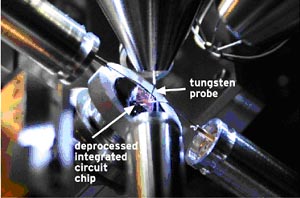
Fig 17: F100 in an FIB at 52 degree tilt
|
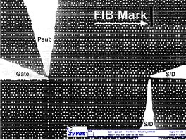
Fig 18: Probe tips "landed" on features
|
Also in April 2004, Zyvex introduced an application note for Manipulation of Collagen for mechanical characterization. Using the Zyvex L100 nanomanipulator system with microgrippers, collagen fibers were actually tied into knots for mechanical characterization (figures 19-21).
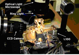
Fig 19: L100 performing collagen fiber manipulation
|
Fig 20 : 4 degree-of-freedom robotic positioner
|
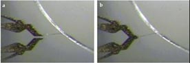
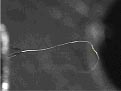
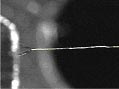
Fig 21 a,b,c,d : Left-to-right: microgrippers grasping collagen fiber, and pulling the fiber taut
|
Click here for a complete list of current published application notes.
Partnerships for Enhanced Capabilities and Rapid Time-to-Market for Customers
In 2003, Zyvex partnered with Keithley Instruments, the leader in electrical measuring equipment. The Zyvex-Keithley partnership delivers an unmatched ability to bring very sharp probes into contact with nanoscale components, and to perform electrical characterization with 1 pico-amp precision. Zyvex and Keithley successfully combined the S100 Nanomanipulator with the model 4200 DC electrical characterization system (Fig. 22) to deliver this capability as the KZ100 nanomanipulator system.
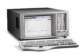
Fig 22: Keithley model 4200 DC Characterization System
|
Also in 2003, Zyvex introduced a formal Partner Program, which has led to partnerships with leading suppliers of SEMs and FIBs to deliver enhanced applications to customers. The Partner Program has also led to partnerships with Distributors around the world, as well as a number of carbon nanotube suppliers for our MATERIALS business line. We believe numerous additional partnerships will emerge in the coming months and years, as nanomanipulators become actual manufacturing systems, with a variety of supporting sub-systems and components that are the core competencies of other firms.
Software Tools
In the pursuit of microscale machines along our downscaling path, we encountered similar gaps in simulation software. We needed software that could more accurately represent what a final MEMS component would look like (including surface characteristics), and how it would perform (Fig 23). We also needed software to simulate the three-dimensional aspects of MEMS assembly (Fig 24). We subsequently developed Memulatorô software using efficient manipulation of voxels. Zyvex and Coventor announced a partnership in 2003 that resulted in a licensing agreement and full implementation of Memulatorô into the Coventor software suite.
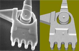
Fig 23: Actual SEM image (left) vs Memulator image
|
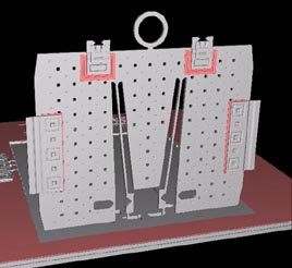
Fig 24: Memulator image of 3D MEMS assembly
Click for larger version
|
From R&D to the Factory Floor
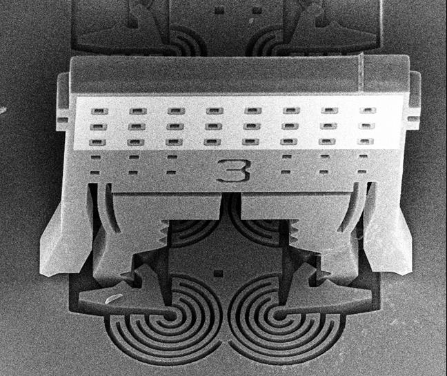
As nanoscale technology developments continue, enabling tools will increasingly take on the role of manufacturing systems, in addition to their current role as tools for R&D and metrology. Also, as the tools become increasingly sophisticated in their ability to assemble and test at the micro and nano scale, they will yield an entirely new class of components that can be assembled into an entirely new class of tools, at increasingly smaller scales. This is what we call our "top down" approach to developing nanoscale technology, and it is the backbone of our five-year $25M NIST-ATP cost-share program. At Zyvex, we have reached the point where the mass assembly of our tools must be enabled by our own tools; it is simply not practical to hand assemble such small systems, and conventional automated assembly is not cost effective.
The objective of the NIST-ATP program is to develop true micro and nano scale assembly "systems." While many of the basic building blocks and techniques for micro assembly have existed for years, complex micro systems require novel assembly methods and techniques. Three-dimensional manufacturing systems require methods to mechanically interlock disparate components from a variety of manufacturing processes. Zyvex has developed such techniques, many of which have been awarded patents (see figures 25-29 below). Additionally, programmable three-dimensional systems require methods to electrically interconnect various components. In building complex micro and nanoscale assembly systems, electrical signals must pass from one axis of motion to another, and reliably deliver the required signals noise-free, in a vacuum environment. The NIST-ATP program is solving these problems as well, with unique solutions and easy-to-assemble interfaces.
Using tools to develop and assemble other tools is not a novel concept, but it has never been done at these scales. Tools building other tools will further enable applied nanotechnology, by continuing to enable cost-effective manipulation of nanoscale components and sub-systems. Mass production of complex micro and nano scale systems will become enabled when the systems are able to work in massively parallel environments, literally assembling thousands or millions of components at a time. This is only feasible if the systems are very small, very inexpensive, and very efficient (see early prototype fig 30).
Fig 25: 300 µm Interlocking connector
|
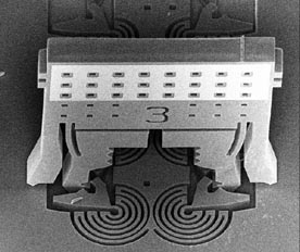
Fig 26: Assembled connector
Click for large version
|
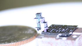
Fig 27 a,b: Assembled MechTileô microsctructure
|
Click for large version
|
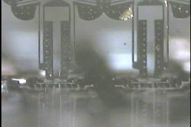
Fig 28: Parallel Assembly; dual pick-up
Click for large version
|
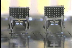
Fig 29: dual place/assemble (300 µm connector)
Click for large version
|
Fig 30 a,b: Early prototype single-axis robotic
actuators (250µm diameter-left; 250µm width-right)
|
|
Nanoscale Assembly
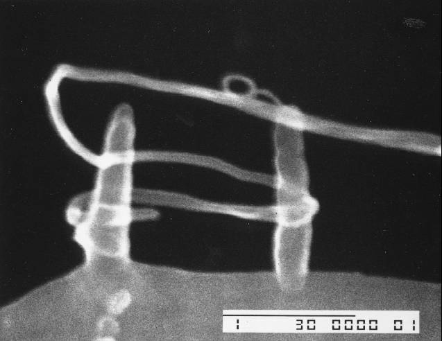
As the machines become smaller, further cost effective downscaling of assembly is enabled. To most cost effectively assemble equipment to perform nanoscale assembly, the equipment will have to be small, inexpensive to produce, and capable of massively parallel assembly. Below are images of a demonstrated process of assembling carbon nanotubes (fig 31).
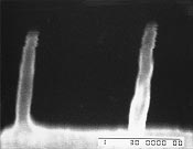


Fig 31 a,b,c: Nanoscale assembly; wrapping carbon nanotubes around posts
Click b & c for large versions
|
Atomically Precise Manufacturing
The ultimate goal of nanoscale technology is atomically precise manufacturing. While Scanning Tunneling Microscopes (STMs) have existed for years, it is not practical to consider any molecular or atomic or even nanoscale manufacturing techniques until the cost and size of the manufacturing equipment are sufficiently reduced. Size and cost reduction are the goals that drive our TOOLS business. Below are simple atomic and molecular manipulations demonstrated in our STM (Fig 32 a,b): executing removal of an individual atom, and controlled manipulation of C60 molecules. As the tools and robotic systems shrink and are able to work in massively parallel assembly lines, operations like these will become commonplace in factories, building atomically precise components and subsystems.
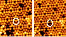
Fig 32 a,b: Repositioning of individual atom
|
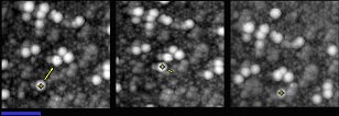
Fig 33: Moving C60 buckeyballs around
|
Summary
The growing field of applied nanotechnology must be enabled by tools that have been developed specifically for nanoscale research and manipulation. Zyvex has an entire business line dedicated to developing these tools and systems for researchers and manufacturers around the world. With a growing list of marquee companies and universities discovering the capabilities of Zyvex's tools, the number of applications enabled by these tools is expanding rapidly. The objective for the Zyvex tools business line is to deliver cost effective solutions for the assembly and test (manual and automated) of components smaller than 3mm, and requiring manipulation to sub-nanometer precision. On a daily basis, we strive to ensure that the equipment is not the limiting factor for our customers. With each new application encountered, we first look to improve the process, then downscale the equipment, and finally integrate the process and equipment into an automated system. Through relentless execution of this continuous cycle, Zyvex intends to one day provide atomically precise nanoscale manufacturing systems.
|
Robert Folaron is the Director of Product Development. He joined Zyvex in November 2002 as the Manager of the Control Engineering Group.
Robert brings more than a decade of successful high-tech corporate leadership and international market start-up successes. He has led teams and companies: to commercialize MEMS technology solutions, provide robotic automation, software solutions, IT systems integration services, manufacturing systems integration, web development, and e-commerce solutions. Robert specializes in commercializing leading edge solutions in emerging markets.
Folaron is named as an inventor on seven U.S. patents, and one European patent, and has published over twelve articles on vision-guided robotics, advanced semiconductor packaging and testing, the commercialization of MEMS, and internet commerce.
He can be reached by email, here
|
Return to Top
TOOL MAKERS SURVEY
By Rocky Rawstern
In this survey, we spoke with companies who make leading edge research tools, and asked them to respond to the following questions:
1. From your point of view, what is nanotechnology?
2. Please talk about the tools your company has developed in the past, and how they enabled research into nanoscience.
3. What tools are you working on today, and what are the specific R&D applications?
4. In your estimation, how big is the market for nanoscience and nanotechnology tools, and how is it growing?
5. In what areas of nanoscience research are improved tools needed most?
6. Considering the rapid pace at which our understanding of nanoscale phenomena is growing, what developments excite you the most?
7. In your opinion, what are the most difficult hurdles yet to be crossed in our understanding of the nanoscale?
Responding were:
Patrick O'Hara - Ambios Technology
Harald Fischer - WITec GmbH
Brian Lim - Atomate Corporation
Vic PeÒa - nanoTITAN
Brian Helfrich - Nano-Hive
Trey Middleton - 4Wave

Patrick O'Hara, CEO of Ambios Technology, Inc.

From your point of view, what is nanotechnology?
Nanotechnology relates to unique technological advancements at length scales less than 100 nm. Also, nanotechnology involves things that are novel and were not possible ten or so years ago.
Please talk about the tools your company has developed in the past, and how they enabled research into nanoscience.
Ambios Technology manufactures surface measurement and visualization tools for the academic and industrial research communities. With systems installed at various national and international preeminent research universities and a variety of industrial and government MEMS and nanotechnology laboratories, our customers are investigating a variety of unique applications. From stress in Uranium films to biometric fluidics, our tools are used to characterize many structures and processes used to advance everything from treatment of diabetes to national security.
What tools are you working on today, and what are the specific R&D applications?
We recently introduced (at Conference on Lasers and Electro Optics - CLEO, May 18, 2004) a tool used to measure surface features as small as .2nm using a novel imaging interferometer. This new tool allows non-contact measurement of a variety of surfaces important to the development of MEMS and nanotechnology structures. The ability to visualize and measure surfaces at this scale allows researchers a previously unavailable mechanism to evaluate their ideas.
In your estimation, how big is the market for nanoscience and nanotechnology tools, and how is it growing?
Although it is difficult to estimate, our market research shows that the market for surface measurement and visualization tools for use in the "nanotechnology" market is presently $115M to $130M and will grow at a compounded annual growth rate of 23% over the next 5 years due to intensive worldwide capital investment.
In what areas of nanoscience research are improved tools needed most?
Process control and development.
Considering the rapid pace at which our understanding of nanoscale phenomena is growing, what developments excite you the most?
I believe that the developments in medical devices and procedures will be absolutely astounding in the coming years as a direct result of efforts by researchers in nanotechnology.
In your opinion, what are the most difficult hurdles yet to be crossed in our understanding of the nanoscale?
Material properties which are easily understood at the macroscopic scale frequently defy intuition at the nanoscale. In order to really move the science forward the basic nature and material properties of the newly developed thin films and nanoscale structures must be better understood.
|
Mr. Patrick O'Hara is the President and CEO of Ambios Technology, Inc., a manufacturer of surface measurement and visualization systems. He has a Bachelor of Science Degree in Physics from the University of Oregon.
Ambios Technology, Inc., headquartered in Santa Cruz, California, is a manufacturer of high performance bench top metrology and visualization equipment for the data storage, semiconductor, general industrial and academic research marketplaces. Additional information on Ambios Technology can be found here.
|
Harald Fischer, Marketing Manager, WITec GmbH.

From your point of view, what is nanotechnology?
In our opinion nanotechnology includes all tools, methods, phenomena and techniques leading to a deeper understanding of nanoscale properties and to a miniaturization of technical equipment providing new and unique kinds of applications.
Please talk about the tools your company has developed in the past, and how they enabled research into nanoscience.
WITec has developed the AlphaSNOM, an easy to use cantilever based near-field scanning optical microscope integrating confocal as well as atomic force microscopy in one instrument. In near-field optical microscopy it is possible to overcome the diffraction limit of optical microscopy leading to high resolution imaging of optical properties of a sample. With the AlphaSNOM the topography is imaged simultaneously with the optical image, not limiting the research to only one technique. To image chemical properties WITec has developed the Confocal Raman Microscopy CRM 200, enabling high resolution Raman microscopy with highest sensitivity. Due to the modular setup of the WITec microscopy system, it is for example possible to upgrade the CRM 200 with AFM capabilities. For atomic force microscopy WITec offers the Mercury 100 AFM with the integrated Digital Pulsed Force Mode, a unique measurement mode for imaging of various surface properties. With modular, high resolution microscopy systems WITec provides universal tools for research and development in nanotechnology and materials science on the nanoscale.
What tools are you working on today, and what are the specific R&D applications?
Today WITec is further developing its existing microscopy systems and is working on improved high resolution imaging modes for materials research which may be important for microelectronics, coating development, surface science, biomedical applications, or nanophotonics.
In your estimation, how big is the market for nanoscience and nanotechnology tools, and how is it growing?
With the raising amount of technical applications in the field of nanotechnology, an adequate growing demand for nanotechnology tools can be expected. This will depend on the quality and the acceptance of the resulting products for technical or consumer applications.
In what areas of nanoscience research are improved tools needed most?
Tools are needed not only to image the samples but also to manipulate or characterize various properties on the nanoscale in order to link nanoscopic effects to macroscopic behavior.
Considering the rapid pace at which our understanding of nanoscale phenomena is growing, what developments excite you the most?
We are mostly exited about the possibilities in designing new materials and components by controlling the nanoscale properties, resulting in dedicated materials for new and unique technical applications.
In your opinion, what are the most difficult hurdles yet to be crossed in our understanding of the nanoscale?
Up to now a deep understanding of phenomena at the nanoscale is already evident. The next more difficult step, requiring a lot of creative efforts, must be not only to observe the nanoscale but also to transfer the knowledge into technical useful applications.
|
Mr. Harald Fischer is a Marketing Manager for WITec GmbH.
WITec is a manufacturer of high performance equipment for scientific and industrial applications focused on new solutions for Optical and Scanning Probe Microscopy (Scanning Near-field Optical Microscopes, Confocal Scanning Microscopes, Raman-CSM, Atomic Force Microscopes, Pulsed Force Mode AFM). WITec offers the AlphaSNOM using unique cantilever technology, the Confocal Raman Microscope CRM 200 designed for highest sensitivity and resolution and the Mercury 100 AFM with the integrated Digital Pulsed Force Mode for material research and nanotechnology. More information is available here.
|

Brian Lim, CEO of Atomate Corporation.

From your point of view, what is nanotechnology?
Nanotechnolgy is an interdisciplinary field that enables products that take advantage of properties that can only be realized with nano-scale materials. At the nanometer scale, physics crosses into the quantum realm and amazing things are possible. A good example of this is the carbon nanotube. A transistor made out of this material has the potential to be two orders of magnitude smaller in size and an order of magnitude faster in operating frequency, while consuming a small fraction of the power of a CMOS transistor. This is not just an incremental improvement, but a technology that breaks through the fundamental physical limits of semiconductors in their current form. The carbon nanotube is also over 100 times stronger than steel and as thermally conductive as diamond. Devices made of such materials will change the world and enable the creation of entirely unforeseen products.
Please talk about the tools your company has developed in the past, and how they enabled research into nanoscience.
Atomate develops solutions for synthesis of nanotubes and nanowires. We offer robust commercial systems, components, and process materials for nanostructure synthesis using the chemical vapor deposition method. Controlled growth of nanostructures is a field that is still very much in the scientific research phase. As new processes are developed, existing equipment quickly reach their limits. We leverage our process knowledge and engineering experience to quickly find solutions that break through these limitations so that interesting scientific discoveries can evolve into products.
What tools are you working on today, and what are the specific R&D applications?
We are currently working on nanostructure characterization instruments in addition to advanced systems for nanowire and nanotube growth. Our new instruments will help our customers characterize the nanostructures grown in our system. We have invented very elegant solutions that improve control over the many variables that affect the quality and repeatability of nanostructure synthesis, and we have integrated a number of safety features, especially for nanowire synthesis where toxic gases are used.
In your estimation, how big is the market for nanoscience and nanotechnology tools, and how is it growing?
We believe that the market for nanoscience and nanotechnology tools is currently about $500 Million per year. I believe that this will grow to over $20 Billion during the next 10-15 years. The National Science Foundation published Societal Implications of Nanoscience and Nanotechnology in March 2001. This document describes how nanotechnology has the potential to produce over $1 Trillion per year in new products by 2010-2015 in materials, electronics, pharmaceuticals, transportation, chemical plants, and energy. A lot of tools will be needed to produce a Trillion Dollars worth of products!
In what areas of nanoscience research are improved tools needed most?
Atomate has helped the nanotechnology researchers with tools that really improve control over the synthesis of nanostructures. Now, we find that characterizing these materials are the bottle neck in the research market. We are planning to launch these tools by Fall, 2004.
Considering the rapid pace at which our understanding of nanoscale phenomena is growing, what developments excite you the most?
The economic impact of nanotechnology can be compared to that of silicon-based semiconductors on the vacuum tube age. What really excites me is the creation of entirely unforeseen products. How many people during the 1980's would have thought that I can take a high resolution digital photograph of my son's first birthday and email it to his uncle on a business trip in Korea with my cell phone? Recently, Stanford University researchers produced 90% semiconducting carbon nanotubes with the CVD process. It is just a matter of time before these nanotubes are used as devices in integrated circuits.
In your opinion, what are the most difficult hurdles yet to be crossed in our understanding of the nanoscale?
Understanding the nanoscale requires solving difficult problems in quantum physics that even the most power computers today cannot solve. Most of the research work is performed empirically. Nanotechnology will eventually enable devices such as quantum computers that may be able to solve these incredibly complex equations. Until such a break through, nanotechnology research will progress with a lot of intelligent guessing and experimentation. Atomate will help improve this experimentation process.
|
Mr. Brian Lim is the CEO of Atomate Corporation. Prior to Atomate, Brian was VP of Business Development at NanoDevices (acquired by Veeco); VP of Engineering at Alpha Virtual; VP of Marketing at Broadware; Director of Marketing for StarOffice; and Product Manager at Sun Microsystems. Brian also engineered mission-critical devices for interplanetary science instruments for 8 years at NASA-JPL. Brian earned a MS in Management and Engineering from the MIT Sloan School of Management and a BSME, also from MIT.
Atomate Corporation develops complete systems, critical components, and special materials optimized for the synthesis of nanotubes and nanowires. Atomate team is dedicated to supplying products that solve problems efficiently and economically. Atomate has a solution for researchers who desire enhancements to existing systems and for those who want to build or buy a new system. Atomate's mission is to develop products that enable the customer to focus their efforts on the science, not on engineering of equipment. Additional information on Ambios Technology can be found here.
|
Vic PeÒa, CEO nanoTITAN, Inc.
From your point of view, what is nanotechnology?
Nanotechnology is the ability to control or manipulate on the atomic scale for the purpose of creating molecular tools. It is a multi-disciplinary process that includes the integration of myriad scientific disciplines and engineering applications in a collaborative fashion towards an economic or societal goal. For nanotechnology to be successful it must incorporate prudent risk engineering principles to insure the safety and security of its end products, but more so, to safeguard the health and stability of the world's people and its environment.
Please talk about the tools your company has developed in the past, and how they enabled research into nanoscience.
nanoTITAN, Inc. was founded three years ago with the expressed mission of being the primary producer and provider of nanoinformatics to the nanotechnology community. We have adopted a Life-Cycle Systems Engineering approach to supporting applied nanoscience and have taken a progressive approach to the development of our software tools for nanodevice design and engineering. nanoTITAN has committed to the exclusive use of Java, because of all its advantages, but most importantly, its architecture neutrality, portability and extensibility.
We started with nanoMLô, a data markup language for the representation and interchange of nanodevice designs. nanoML is the first and only mark-up language exclusively dedicated to nanoscience and technology collaboration and communication. nanoML is freely available and has been downloaded and used worldwide for the communication of nanoscience and, specifically, the interdisciplinary exchange of information regarding nanoscience and technology.
Following the release of nanoML, we released nVisualizerô, our powerful visualization engine. nVisualizer provides state-of-the-art interactive 3D displays for our nanotechnology products and is also applicable across the entire range of science, technology and business in general.
In September 2003, we released the first three capabilities to our flagship software product, nanoXplorerô -- Display, Design and Database. These capabilities allow the nanodevice researcher to attribute, characterize and design his mind's eye concept, all the while being able to see - visualize - the evolving maturity of his or her development. The Database capability allows the nanodevice developer to upload his/her design for peer review, or to download similar research that may impact on his/her concept.
What tools are you working on today, and what are the specific R&D applications?
We are presently striving for a June, 2004 release of our much-anticipated Simulation capability that will provide the next function in the Life Cycle approach to our nanoXplorer suite. Our Simulation capability, seamlessly integrated with the Display, Design and Database components will allow the nanoscientist to progress from concept to design, peer review, and simulation, all by using a single platform, at a single low cost, and low risk investment.
What all this means is that the nanoscientist has at his/her disposal a toolkit that allows not only the interdisciplinary research and development of his/her concept, but the ability to share collaboratively the evolvement of the nanodevice project with peers worldwide. This concept is new to the nanoscience R&D community and is built on the foundations set by nanoML, which is incorporated in nanoXplorer.
In your estimation, how big is the market for nanoscience and nanotechnology tools, and how is it growing?
There are two fundamental areas in nanoscience and nanotechnology tools, hardware, such as microscopy, and software, such as design, engineering and modeling and simulation tools, what we call "nanoinformatics." These two areas are growing quite rapidly and will continue to grow at an accelerating pace as progress is made in R&D, and commercialization starts occurring, and more and more investment capital enters the nanotechnology sector.
The National Science Foundation is quoted often for projecting a worldwide market in nanotechnology of $1 Trillion by 2015. Of this, we estimate that the demand for nanotechnology tools, both hardware and software will account for at least 30% on the conservative side to as large as 50% of the total capital investment in nanotechnology businesses. A critical aspect of this is going to be the demand for human resources - HR - to operate the tools, but this is not part of this discussion.
At the present time, much of the demand for tools is still emerging. We see it beginning to accelerate by the end of 2004, and continue a sharp and sustained increase. We expect this to be especially true in the software tools sector, where demand will increase proportional to the cost of entry of business to nanotechnology and of the cost of producing nanodevices. Another emerging requirement for robust nanoinformatics is the need to conduct systems engineering based simulations of risk analysis in nanodevice development against various scenarios in health, safety, security, and environmental impacts in the development of nanotechnology products. In our opinion, this is an underdeveloped area of research that is beginning to emerge and will soon command worldwide attention and funding.
In what areas of nanoscience research are improved tools needed most?
We would like to focus our response to this question solely on the requirements for nanoinformatics and computational sciences. As new concepts in nanodevices are put forth, application feasibility will have to be explored to include investments in intellectual and human resources, capital formation, market analysis, environmental impacts, societal and workforce implications, and policy and legal issues. Powerful, accurate, and timely modeling and simulation tools, and data processing capabilities beyond what is currently available will have to be used to address these issues before full-scale production and consumption of nanodevices can be achieved. While nanoscience and technology hold tremendous promise, economical, ethical and scientific decisions must be weighed against the best data and information available before committing to full scale productions.
Considering the rapid pace at which our understanding of nanoscale phenomena is growing, what developments excite you the most?
The most exciting developments in the nanoscale phenomena will be in the areas of medicine and pharmacology. While I have not addressed the attainment of nanoscale convergence of nanomaterials, biotechnology, and computational science, the integration or convergence and subsequent "emergence" of nanodevices for the good of mankind is clearly the most exciting. Other more near term applications are also worthy of investment, but none more so than that which can make the human experience healthier and disease free.
In your opinion, what are the most difficult hurdles yet to be crossed in our understanding of the nanoscale?
I am concerned that the risks of nanoscale research and development--and the understanding, management and mitigation of those risks as they impact society and the world environment--have not been fully explored, debated, and resolved. In a previous article I recommended that a Tenth Grand Challenge be added to the National Nanotechnology Initiative's "Grand Challenges" and that it should be "Development of Meaningful and Enforceable Standards of Security, Ethics and Societal Factors." Of necessity, this Tenth Grand Challenge would have to address risks and their mitigation and management on a global scale. I further recommended a World Body Convention such as the Geneva Convention be formed for the purpose of developing a framework for the safe and secure development of nanotechnology.
|
Mr. Vic PeÒa is Co-Founder and Chief Executive Officer of nanoTITAN, Incorporated, an emerging nanoinformatics company specializing in design and engineering software for the nanotechnology industry. He is instrumental in the business development of the company and its presence in the nanotechnology industry.
He is a member of the President's Council of Advisers in Science and Technology --Nanotechnology Technical Advisory Group; Co-Chairman of the Northern Virginia Technology Council's Nanotechnology Committee; and a founding member of the Initiative for Nanotechnology in Virginia, INanoVA.
nanoTITAN is the premier provider and developer of state-of-the-art design, engineering, simulation, database and assembly software for research and development in nanoscience and nanotechnology. nanoTITAN's nanoinformatics products and services offer nanotechnology researchers and developers resource-enhancing alternatives to creating concurrent and proprietary software to realize their concepts. The company is dedicated to being a trusted partner in the concept-to-commercialization of molecular nanotechnology efforts in academia, business, and government.
|
Brian Helfrich, Systems Architect, Nano-Hive

From your point of view, what is nanotechnology?
Nanotechnology is the next step in the general and ultimately arbitrary manipulation of all aspects of our world. It's a growing expectation shrouded in a growing influence on our lives. It creeps into our reality like the fog into San Francisco at dusk after a sunny day; growing more and more tangible as it becomes part of the ambiance of the night. Through that same misty curtain we may expect something new and fanciful to emerge as we press on through the streets, or even fear a dark threat looming ahead. Either way, the benefits and augmentation of nanotech to our lives will continue to embrace us and allow us to speculate and anticipate further and further past what we can imagine today.
Please talk about the tools your company has developed in the past, and how they enabled research into nanoscience.
We're a relatively new company just beginning to make our way in the market.
What tools are you working on today, and what are the specific R&D applications?
We're working on a simulator specifically designed for nanotech research and development. Simulation is crucial in nanotech as physical experiments may be too costly, too numerous, too dangerous, or even impossible to perform. Applications of the simulator include exploration of nanodevice designs and behaviors, characterization of nanodevices, nanotech education, and providing part of a standard means for communicating results and processes.
The simulator is being developed as an open source project with a very modular, plugin-based architecture. We're targeting it as a simulation platform into which researchers and developers can plugin, or develop, the specific modules they need. Researchers developing new simulation code can confine their efforts to writing a plugin to implement their ideas while getting the rest of the simulator, such as data storage and data input/output, for free (with respect to development effort.)
In your estimation, how big is the market for nanoscience and nanotechnology tools, and how is it growing?
Today I would liken the market for nanotech tools to that of microtech tools. Currently there's still a lot of retrofitting microtech tools, like measurement instruments and manipulators, towards nanotech purposes. There aren't a lot of companies like Zyvex, who are building nanotech tools from scratch. The market for nanotech tools will change as we explore, discover, and understand what nanotech tools are, but I anticipate the market to be similar to what microtech is today, heavy on the fabrication plant side.
In what areas of nanoscience research are improved tools needed most?
Some of the big problems with today's simulators are that they're quite difficult to use, expensive, and they often are only useful for a specific problem. Many labs build their own simulation capability from scratch because of these reasons. The problem is that it forces them into a tier of software development and computing they may not want to be in, and they may have to forgo some desirable simulation capabilities because of time and effort. Nano-Hive addresses this by being easy-to-use, free, and very extensible.
Considering the rapid pace at which our understanding of nanoscale phenomena is growing, what developments excite you the most?
Nanotubes exhibit so many desirable structural properties; I'm very keen to see them used in automobiles, aircraft, and buildings. I think the doors that nanotube materials will open to designers will result in a new echelon of industrial art.
In your opinion, what are the most difficult hurdles yet to be crossed in our understanding of the nanoscale?
Incorporation of direct nanoscale manipulation and assembly into today's industrial processes will be a tough nut to crack and require a new breed of hybrid industrial engineer/scientist.
|
Nano-Hive LLC, located in New York City, NY, develops a modular simulator used for modeling the physical world at a nanometer scale. The intended purpose of the simulator is to act as a tool for the study, experimentation, and development of nanotech entities. Nano-Hive is a GPL/LGPL licensed open-source development and can be downloaded and used for free. Nano-Hive can be run stand-alone, or easily integrated to support other applications such as CAD tools.
|
Trey Middleton, 4Wave

From your point of view, what is nanotechnology?
Research and technology development at the atomic, molecular or macromolecular levels, in the length scale of approximately 1 - 100 nanometer range.
Creating and using structures, devices and systems that have novel properties and functions because of their small and/or intermediate size.
Ability to control or manipulate on the atomic scale.
Please talk about the tools your company has developed in the past, and how they enabled research into nanoscience.
4Wave has developed thin film processing systems utilizing ion beam plasma systems. Such processing systems are used to develop thin films, both single layer films and multi-layer structures.
What tools are you working on today, and what are the specific R&D applications?
Atomic Layer Engineering process equipment, through ion beam innovations. Specifically in two areas - 1) thin film deposition of single material, as well as binary and ternary films through biased target ion beam deposition and 2) thin film etching through low energy (10 - 200 eV) etching techniques.
In your estimation, how big is the market for nanoscience and nanotechnology tools, and how is it growing?
4Wave's addressable market for nanoscience and nanotechnology tools is estimated to be a $50M market today, growing to a $750M market in the next five (5) years.
In what areas of nanoscience research are improved tools needed most?
Nanoscience research can be divided into four (4) sub-categories: 1) Thin Films, 2) Nanotubes, 3) Nanoparticles and 4) Sol-Gels. 4Wave believes each of these areas equally require improved tools, and feels the area of thin film materials can be better served with improvement in metrology techniques for thin film structure evaluation.
Considering the rapid pace at which our understanding of nanoscale phenomena is growing, what developments excite you the most?
The national attention to nanotechnology and the budgets planned for research and development.
In your opinion, what are the most difficult hurdles yet to be crossed in our understanding of the nanoscale?
The transition of nanotechnology research into manufactured products.
|
4Wave provides advanced thin film technologies used in the production of nanometer-scale components in the computer and telecommunications industries. 4Wave's unique technologies enable the fabrication of thin film materials at the atomic scale, with unprecedented levels of precision and functionality using robust, cost-effective equipment. Atomically engineered thin-film devices are foundational to future integrated circuit memory elements, integrated circuit transistors, extreme ultraviolet lithography masks, disk-drive heads, and telecommunications lasers.
|
Nanosys: To IPO or Not to IPO? Is That the Question? |
 |
|
The industries that nanotechnology will likely have a disruptive effect on in the near term include the following:
(Amounts are Billions of US Dollars)
|
$1,700 |
Healthcare |
|
$600 |
Long Term Care |
|
$550 |
Electronics |
|
$550 |
Telecom |
|
$480 |
Packaging |
|
$450 |
U.S. Chemical |
|
$460 |
Plastics |
|
$182 |
Apparel |
|
$180 |
Pharmaceutical |
|
$165 |
Tobacco |
|
$100 |
Semiconductor |
|
$92 |
Hospitality / Restaurant |
|
$90 |
US Insurance |
|
$83 |
Printing |
|
$80 |
Corrosion Removal |
|
$57 |
US Steel |
|
$43 |
Newspaper |
|
$42 |
Diet Supplement |
|
$40 |
Diet |
|
$32 |
Publishing |
|
$30 |
Catalysts |
|
$27 |
Glass |
|
$24 |
Advertising |
|
$18 |
Cosmetics |
|
$13 |
Chocolate |
|
$10 |
Battery |
|
$5 |
Blue Jeans |
|
$4 |
Khakis |
|
$2.8 |
Fluorescent Tagging |
|

The Mother of All Minds
Dudley Lynch


Our Review
The Superswarm Interview
The Superswarm Option
Nanoveau - This column will cover the science, the speculation, and (occasionally) the politics of nanotechnology and related topics. If you want to know what nanotech is about, and how and why it will change everything we know-Nanoveau is for you.
|
|
On April 23rd, 2004, Nanosys announced their plans to raise up to $115 million in an IPO so that it can further expand its research across a range of nanotechnology businesses, according to the filing with the Securities and Exchange Commission. Nanosys said it had applied to list on Nasdaq under the symbol "NNSY" (Nasdaq").
This and Nanosys does not even have revenues or a product yet even though they do have IP. Yet if the company manages a successful listing, its strategy is a high-risk, high-reward one that will pay off only if the technology and resulting building blocks are adopted as an industry standard in certain niches. Nanosys will make some money in the future but not nearly as much as hoped. News of disappointed investors in Nanosys's stock performance will make it all the more difficult for more viable nanotech startups to raise funding or go IPO. That is not to say there will not be any lucrative nanotech IPO's but Nanosys isn't it.
For those who buy Nanosys IPO shares, they will soon realize they've been had, but by whom? Was too much funding given to an overvalued Nanosys? Might current investors be unloading it onto the unsuspecting public via an IPO in order to recoup their investment? These are some hard questions that need to be asked so let's take a look at some numbers and at their current situation with a critical eye.
Nanotechnology has been a hot sector among venture capitalists. "It's been very eagerly awaited by the nanotech business community,'' said David Forman, a staff writer at Small Times magazine, a nanotechnology journal in Ann Arbor, Mich. "They are looked at as the poster child of nanotechnology, and people are looking to them to legitimize the field on Wall Street.''
The Nanosys IPO will not legitimize the field on Wall St as many in the nanotech industry hope. What it will do is what the failed dot.com and biotech IPO's did for their industries a few years back which is cause many VC's to lose a lot of money due to unrealized returns.
This past June 3, 2003, Nanosys led most nanotech startups in capturing venture capital investments, closing $38 million in financing for a total of $70 million in equity and non-equity funding since its founding two years before. That fundraising event garnered much publicity as Nanosys closed its second round first at $30 million on April 24th, 2003, almost exactly a year before the IPO announcement, before opening that second round back up for an additional $8 million that closed on June 3rd, 2003.
Investors ARCH Venture Partners, CW Group, Polaris Venture Partners, Venrock Associates, Prospect Venture Partners and Alexandria Real Estate Equities also participated in the last financing round; they are joined in this round by CDIB BioScience Ventures, Chiao Tung Bank, China Development Industrial Bank, Harris & Harris, Lux Capital, Quanta Computer and SAIC Venture Capital Corp. Existing investors that also participated included ARCH Venture Partners, CW Group, Polaris Venture Partners, Venrock Associates, Prospect Venture Partners, and Alexandria Real Estate Equities.
Chief Executive Larry Bock confirmed that the additional $8 million comes from new investors UOB Hermes Asia Technology Fund, UOB Venture Technology Investments Ltd., Healthcare Focus Fund L.P., Eastman Kodak Co, H.B. Fuller Co. and others. The UOB funds are managed by UOB Venture Management Pte Ltd., a subsidiary of United Overseas Bank of Singapore. The Healthcare Focus Fund is managed by Arch Venture Partners for the California Public Employees Retirement System (CalPERS) . Kodak and Fuller participated as strategic investors.
According to several of the investors who managed to win a spot in syndicate, no fewer than 65 investors lined up for a piece of the company. According to an article by Tyson Freeman in May 2003, "The competition helped bid the company's valuation up nearly 75%, says Nanosys CEO Larry Bock."
Company valuations shouldn't be based on something as subjective as competition between investors and in this case, perceived value or desperation to get in on a lucrative deal lead by high profile VC's. I don't think anywhere in a valuation course is investor competition a variable. Were the dot.com and biotech bubbles so long ago?
In July 2004, Nanosys will be about 3 years old. A year before its IPO announcement, Nanosys President and CEO Larry Bock said the new $38 million second round investment would enhance Nanosys' development and marketing efforts for its portfolio of nanotechnology-enabled products in chemical and biological sensing, photovoltaic and high-performance macroelectronics. The $115 million IPO is so that it can further expand its research across a range of nanotechnology businesses.
What happened during that year after raising $38 million for a total of $70 million in financing that justifies another $115 million? Are we actually going to see some product and sales? As of Dec. 31, 2003, Nanosys had $39 million in cash. Do they really need more money?
Since its founding in July of 2001, Nanosys has lost $17 million. In 2003, Nanosys had a loss of $9.2 million on revenues of $3 million, compared with a loss of $7.1 million a year earlier on revenues of $283,000, according to its regulatory filing. However, most of the revenue currently derives from conducting research. In-Q-Tel, for instance, has agreed to pay Nanosys up to $3 million for research, while Intel has made a similar commitment for $1.9 million.
Plus, the company is not selling products yet and they admit it. Designing commercially viable molecules takes years, and the company will probably have to contend with larger competitors and other start-ups, regulatory changes, public suspicion of nanotechnology and intellectual property disputes, according to Nanosys.
And they still admit it. "To date, we have not successfully developed any commercially available products," the company wrote in the S-1 form it filed with the SEC. "We are currently in the investigation phase of all of our potential products. We do not anticipate that our first products will be commercially available for at least several years, if at all."
The company has licensed dozens of patents from key university researchers -- many of whom have joined the company -- in an attempt to create products across a wide number of industries. Those licensing deals and Nanosys' own patents have enabled them to strike joint development deals with Intel; several government agencies; DuPont; and IN-Q-Tel, the firm started by the CIA; to name a few. It also has licensing agreements that allow it to try to commercialize intellectual property coming out of labs at Harvard, the Massachusetts Institute of Technology, the Hebrew University of Jerusalem and other institutions. DuPont wants to use nanotechnology to create thin, flexible display screens. Matsushita hopes to create a new kind of solar panel with Nanosys, and Intel is tapping Nanosys to develop new kinds of memory chips that store data permanently.
As a company, Nanosys remains small. It has 34 employees in a small building in Palo Alto that resembles a research laboratory. The labs are filled with chemical vials connected by clear plastic tubes and powerful microscopes that can show details of the atoms that the scientists are manipulating.
Nanosys' products include nanowires, nanorods, nanotetrapods and nanodots formed from semiconductor materials. Applications include chemical and biological sensors, high-performance large-area macroelectronics and lightweight high-efficiency conformal photovoltaics. Among the ideas is to create a kind of super-velcro that could allow a person to walk up a glass wall. This all sounds very interesting for a research group but unfocused for a company that is supposed to be in business making money.
For a 35-employee startup with no product, and $70 million in investments over 2 years, is $1 million per employee per year with no real product justifiable? Sounds like Nanosys could be overvalued, extremely overvalued.
Nanosys was started by a team of researchers in July 2001 that included MIT veteran Stephen Empedocles. Executive Chairman of the Board of Directors, Larry Bock, a biotech entrepreneur who has started more than a dozen companies, joined Nanosys in October 2001. He and CEO Calvin Chow assembled a star-studded cast of scientists, board members and backers. Several team members are from a successful biotech startup, Calipers Technologies, including CEO Calvin Chow (also ex-Hewlett-Packard), CTO J. Wallace Parce, Ph.D., and VP of IP Michael Murphy.
Nanosys also has an all-star studded Scientific Advisory Board with Harvard's Professor of Chemistry Charles Lieber, along with Paul Alivisatos, a University of California professor who also directs the Molecular Foundry, a multimillion dollar research effort funded by the Department of Energy. Other Scientific Advisory Board members are professors from MIT, Harvard, CalTech, UC Berkeley, Columbia U, UChicago, etc. with heavyweights on the Advisory Board such as John Young, an ex-CEO of Hewlett-Packard, and Greg Yurek, ex-CEO of American Superconductor Corp., and Christoph Westphal from Polaris Ventures who is an M.D. with a Ph.D. in Genetics and is also an ex-McKinsey consultant. Co-founder and Director of Chemistry, Chunming Niu was a post-doc of Charles Lieber's.
Technically speaking, Nanosys seems like a very expensive research incubator with a management team who are very marketing savvy and able to dazzle investors with their vision and pedigrees. They are brilliant at selling themselves even though they're not selling products.
With its great marketing strategy, Nanosys has also been honest about the fact that they will not have products for several years, and that the company may have to contend with larger competitors and other start-ups, regulatory changes, public suspicion of nanotechnology and intellectual property disputes.
Typically VC's don't fund companies at such early stages with no real product or sales. Have the VC's finally realized that in their zeal they came in too early and they paid too much for Nanosys? Remember what happened to dot.com companies? Perhaps an IPO is their way to recoup their investment and pass on their mistake to the public?
Interestingly enough, the money in nanotech won't be made from IPO's. If you look at the many big corporations working in the nanotech sector, such as HP, DuPont, Intel, IBM, etc., the money will be made from M&A (Mergers & Acquisitions) and licensing deals between them and nanotech startup companies.
Stay tuned for next month's article.
|
Dr. Pearl Chin has an MBA from Cornell, a Ph.D. in Materials Science and Engineering from University of Delaware's Center for Composite Materials and B.E. in Chemical Engineering from The Cooper Union.
Dr. Chin specializes in advising on nanotechnology investment opportunities. She is also CEO of Red Seraphim Consulting where she advises investment firms and startup firms on the business strategy of nanotechnology investments. She was Managing Director of the US offices and co-Managing Director of the London offices of Cientifica. Prior to that, she was a Management Consultant with Pittiglio Rabin Todd & McGrath (PRTM)'s Chemicals, Engineered Materials and Packaged Goods group.
Dr. Chin will be advising the Cornell University JGSM's student run VC fund, Big Red Venture Fund (BRVF), on investing in nanotechnology.
She is a Senior Associate of The Foresight Institute in the US and was the US Representative of the Institute of Nanotechnology in the UK. She was an alternate finalist for a Congressional Fellowship with the Materials Research Society.
She was also a Guest Scientist collaborating with the National Institute of Standards & Technology (NIST) Polymer Division's Electronic Materials Group under the US Department of Commerce.
Dr. Chin is a US Citizen born and raised in New York City.
She can be contacted here.
|
Return to Top
In closing, these quotes:
Computational nanotechnology modeling using quantum mechanics, classical atomistic methods and/or mesoscale simulations enable scientists to visualize and predict behavior emerging at length scales of up to 100nm, the realm of nanotechnology. Nanotechnology Software Solutions Accelrys
According to a soon-to-be-released report from Business Communications Company, Inc., RGB-283 Tools and Instrumentation for Nanotechnology, the worldwide market for nanotechnology instruments and tools is estimated at $199.2 million in 2003. Expected to grow at an average annual growth rate of 28.6%, this market is forecast to cross $700 million by 2008. ... Atomic force microscopes dominate the sector-they are expensive, but have applications in almost every nanotechnology field. Indeed, they can be a key component in nanolithography and nanofabrication systems. Expansion of sales of AFMs will be a belle weather for the rest of the nanotechnology industry. We expect the microscopy sector to expand at about 22.4% AAGR. Worldwide market for nanotechnology instruments and tools to cross $700 million by 2008 a report from Business Communications Company, Inc.
Nanotech Tools are instruments and software which allow us to see, touch, manipulate, manufacture, model and simulate in the nanoworld. This is the most mature sector of the nanotech world, including many publicly-traded companies. Now it is more important than ever for the tools to take a leap in capability in order to effectively support the explosion in nanotechnology which is anticipated over time. Nanotechnology Tools- The Picks and Shovels of the Revolution SDForum
Historically, many scientific advances occur only after suitable investigative instruments become available. Today, tools such as the Atomic Force Microscope (AFM) and the Scanning Electron Microscope (SEM) help nanotech researchers visualize, resolve, and perform surface characterization of nanoscale objects. The information obtained with these tools allows
researchers to manipulate atoms and molecules to create new materials and structures. However, tools are needed to measure phenomena going on beneath the surfaces of nanomaterials. Sensitive Electrical Measurement Tools Crucial
In Meeting Nanotechnology's Grand Challenge (PDF) Jonathan L. Tucker, Keithley Instruments, Inc.
The challenges for scientists and engineers working in the area of nanotechnology are complex. The subject area is broad and quite often, interdisciplinary. The scientific work is at dimensional scale where tools for creation, characterization, and visualization are limited, and whose scaling up for large-scale use requires improvements in speed, reproducibility, and control. Tools and metrology are therefore an important an barrier in progress of nanotechnology. Japan-US Symposium Tools and Metrology for Nanotechnology National Nanofabrication Users Network (NNUN) hosted event.
Instruments, tools and nanofacilities are the bottleneck for the industrialisation of the nanotechnology. Companies in this field will be the most important part of the future nanoindustry. The recent rapid advances in nanotechnology are due in large part to our newly acquired ability to measure and manipulate individual structures on the nanoscale. The scanning probes, optical tweezers and other new tools enable the research workers in science and technology to create new structures , measure new phenomena, and explore new applications. In the next years the development of the tools, instruments and services will further act as the main catalyst of the nano-industries. At the same time, the broader applications of nanotechnology will reciprocally strengthen the surge of the tools, instruments and services. Instruments and Tools for Nanotechnology 2003-2006-2010-2015
Market, Technology and Developments for Instruments, Tools, Automation, Information and Service. Helmut Kaiser Consultancy.
From Our Molecular Future, by Douglas Mulhall:
-
What happens to the monetary system when everyone is able to satisfy his own basic material needs at very low cost?
-
How would we use cash when digital manufacturing makes it impossible to differentiate a counterfeit bill or coin from the real thing?
-
What happens to fiscal policy when digital information, moving at light speed, is the major commodity?
-
How fast will monetary cycles move compared to, say, the ten- or twenty-year cycles of the late twentieth century, when products and patents go out of date in a matter of months instead of years?
-
What happens when we don't have to worry about trade or social services for our basic needs, because most of what we need is provided locally with digital manufacturing, and the biggest trade is in information?
-
How do we control the excesses of the ultrarich, the overabundance of the molecular assembler economy, and the challenge to intellectual property laws created by intelligent, inventive machines?
-
What happens if half of all jobs are made redundant every decade?
-
What happens to the War on Drugs when there's no import, export, or transport of contraband because drugs can be manufactured in a desktop machine using pirated software downloaded from the Internet?
-
What happens to democratic controls when individuals can get as rich as small governments in a year or so?
-
What's the relevance of insurance if many things are replaceable at very low capital cost, but liabilities from software are potentially unlimited?
-
How should organized labor react when molecular assemblers and intelligent robots eliminate most manufacturing jobs?
-
What is the nature of work going to be?
-
What happens to land prices when an individual can build a tropical farm under a bubble in North Dakota, and get there from New York in an hour?
-
What happens when everyone can go everywhere, whenever they want, and work from wherever they want?
Return to Top
USEFUL LINKS
For further research, here are pages we found valuable:
Nanotechnology tools for functional proteomics analysis (PDF)
Free Molecular Visualization Tools
Our Tool Makers Directory
Return to Top
IN THE NEXT ISSUE
Issue #13 will cover Memory & Chip Technology. It will land in your mailbox July 5th, 2004.
Infamous Quotes:
"This 'telephone' has too many shortcomings to be seriously considered as a means of communication. The device is inherently of no value to us." Western Union internal memo, 1876
"Heavier-than-air flying machines are impossible." - Physicist and mathematician Lord Kelvin, President of the British Royal Society, 1895
"Everything that can be invented has been invented." - Charles H. Duell, Director of U.S. Patent Office, 1899
"There is no likelihood man can ever tap the power of the atom." - Robert Milikan, Nobel Laureate in Physics, 1923
"Theoretically, television may be feasible, but I consider it an impossibility-a development which we should waste little time dreaming about." - Lee de Forest, inventor of the cathode ray tube, 1926
"I think there is a world market for maybe five computers." IBM's Thomas Watson, 1943
"Landing and moving around on the moon offer so many serious problems for human beings that it may take science another 200 years to lick them." - Science Digest, August 1948
"Computers in the future may weigh no more than 1.5 tons." Popular Mechanics, 1949
"There is no reason anyone would want a computer in their home." Ken Olsen, Digital Equipment Corp, 1977
And the lesson is? It's a tough game to call.
Need advice? Check out NanoStrategies
© Copyright 1999-2004 7thWave, Inc. All rights reserved. More information on copyright, and disclaimers regarding the content of this newsletter can be found here
|


