Home > Press > How flawed diamonds 'lead' to flawless quantum networks
 |
| CREDIT Tokyo Tech |
Abstract:
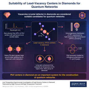
The color in a diamond comes from a defect, or “vacancy,” where there is a missing carbon atom in the crystal lattice. Vacancies have long been of interest to electronics researchers because they can be used as ‘quantum nodes’ or points that make up a quantum network for the transfer of data. One of the ways of introducing a defect into a diamond is by implanting it with other elements, like nitrogen, silicon, or tin. In a recent study published in ACS Photonics, scientists from Japan demonstrate that lead-vacancy centers in diamond have the right properties to function as quantum nodes. “The use of a heavy group IV atom like lead is a simple strategy to realize superior spin properties at increased temperatures, but previous studies have not been consistent in determining the optical properties of lead-vacancy centers accurately,” says Associate Professor Takayuki Iwasaki of Tokyo Institute of Technology (Tokyo Tech), who led the study.
How flawed diamonds 'lead' to flawless quantum networks
Tokyo, Japan | Posted on October 1st, 2021The three critical properties researchers look for in a potential quantum node are symmetry, spin coherence time, and zero phonon lines (ZPLs), or electronic transition lines that do not affect “phonons,” the quanta of crystal lattice vibrations. Symmetry provides insight into how to control spin (rotational velocity of subatomic particles like electrons), coherence refers to an identicalness in the wave nature of two particles, and ZPLs describe the optical quality of the crystal.
The researchers fabricated the lead-vacancies in diamond and then subjected the crystal to high pressure and high temperature. They then studied the lead vacancies using photoluminescence spectroscopy, a technique that allows you to read the optical properties and to estimate the spin properties. They found that the lead-vacancies had a type of dihedral symmetry, which is appropriate for the construction of quantum networks. They also found that the system showed a large “ground state splitting,” a property that contributes to the coherence of the system. Finally, they saw that the high-pressure high-temperature treatment they inflicted upon the crystals suppressed inhomogeneous distribution of ZPLs by recovering the damage done to the crystal lattice during the implantation process. A simple calculation showed that lead-vacancies had a long spin coherence time at a higher temperature (9K) than previous systems with silicon and tin vacancies.
“The simulation we presented in our study seems to suggest that the lead-vacancy center will likely be an essential system for creating a quantum light-matter interface—one of the key elements in the application of quantum networks,” concludes an optimistic Dr. Iwasaki.
This study paves the way for the future development of large (defective) diamond wafers and thin (defective) diamond films with reliable properties for quantum network applications.
####
For more information, please click here
Contacts:
Kazuhide Hasegawa
Tokyo Institute of Technology
Copyright © Tokyo Institute of Technology
If you have a comment, please Contact us.Issuers of news releases, not 7th Wave, Inc. or Nanotechnology Now, are solely responsible for the accuracy of the content.
Bookmark:


| Related Links |
| Related News Press |
News and information
![]() Simulating magnetization in a Heisenberg quantum spin chain April 5th, 2024
Simulating magnetization in a Heisenberg quantum spin chain April 5th, 2024
![]() NRL charters Navy’s quantum inertial navigation path to reduce drift April 5th, 2024
NRL charters Navy’s quantum inertial navigation path to reduce drift April 5th, 2024
![]() Discovery points path to flash-like memory for storing qubits: Rice find could hasten development of nonvolatile quantum memory April 5th, 2024
Discovery points path to flash-like memory for storing qubits: Rice find could hasten development of nonvolatile quantum memory April 5th, 2024
![]() Good as gold - improving infectious disease testing with gold nanoparticles April 5th, 2024
Good as gold - improving infectious disease testing with gold nanoparticles April 5th, 2024
Quantum communication
![]() With VECSELs towards the quantum internet Fraunhofer: IAF achieves record output power with VECSEL for quantum frequency converters April 5th, 2024
With VECSELs towards the quantum internet Fraunhofer: IAF achieves record output power with VECSEL for quantum frequency converters April 5th, 2024
![]() Researchers’ approach may protect quantum computers from attacks March 8th, 2024
Researchers’ approach may protect quantum computers from attacks March 8th, 2024
![]() HKUST researchers develop new integration technique for efficient coupling of III-V and silicon February 16th, 2024
HKUST researchers develop new integration technique for efficient coupling of III-V and silicon February 16th, 2024
Possible Futures
![]() Discovery points path to flash-like memory for storing qubits: Rice find could hasten development of nonvolatile quantum memory April 5th, 2024
Discovery points path to flash-like memory for storing qubits: Rice find could hasten development of nonvolatile quantum memory April 5th, 2024
![]() With VECSELs towards the quantum internet Fraunhofer: IAF achieves record output power with VECSEL for quantum frequency converters April 5th, 2024
With VECSELs towards the quantum internet Fraunhofer: IAF achieves record output power with VECSEL for quantum frequency converters April 5th, 2024
Chip Technology
![]() Discovery points path to flash-like memory for storing qubits: Rice find could hasten development of nonvolatile quantum memory April 5th, 2024
Discovery points path to flash-like memory for storing qubits: Rice find could hasten development of nonvolatile quantum memory April 5th, 2024
![]() Utilizing palladium for addressing contact issues of buried oxide thin film transistors April 5th, 2024
Utilizing palladium for addressing contact issues of buried oxide thin film transistors April 5th, 2024
![]() HKUST researchers develop new integration technique for efficient coupling of III-V and silicon February 16th, 2024
HKUST researchers develop new integration technique for efficient coupling of III-V and silicon February 16th, 2024
Discoveries
![]() Chemical reactions can scramble quantum information as well as black holes April 5th, 2024
Chemical reactions can scramble quantum information as well as black holes April 5th, 2024
![]() New micromaterial releases nanoparticles that selectively destroy cancer cells April 5th, 2024
New micromaterial releases nanoparticles that selectively destroy cancer cells April 5th, 2024
![]() Utilizing palladium for addressing contact issues of buried oxide thin film transistors April 5th, 2024
Utilizing palladium for addressing contact issues of buried oxide thin film transistors April 5th, 2024
Announcements
![]() NRL charters Navy’s quantum inertial navigation path to reduce drift April 5th, 2024
NRL charters Navy’s quantum inertial navigation path to reduce drift April 5th, 2024
![]() Discovery points path to flash-like memory for storing qubits: Rice find could hasten development of nonvolatile quantum memory April 5th, 2024
Discovery points path to flash-like memory for storing qubits: Rice find could hasten development of nonvolatile quantum memory April 5th, 2024
Interviews/Book Reviews/Essays/Reports/Podcasts/Journals/White papers/Posters
![]() Simulating magnetization in a Heisenberg quantum spin chain April 5th, 2024
Simulating magnetization in a Heisenberg quantum spin chain April 5th, 2024
![]() Discovery points path to flash-like memory for storing qubits: Rice find could hasten development of nonvolatile quantum memory April 5th, 2024
Discovery points path to flash-like memory for storing qubits: Rice find could hasten development of nonvolatile quantum memory April 5th, 2024
|
|
||
|
|
||
| The latest news from around the world, FREE | ||
|
|
||
|
|
||
| Premium Products | ||
|
|
||
|
Only the news you want to read!
Learn More |
||
|
|
||
|
Full-service, expert consulting
Learn More |
||
|
|
||