Home > Press > Engineering the boundary between 2D and 3D materials: Cutting-edge microscope helps reveal ways to control the electronic properties of atomically thin materials
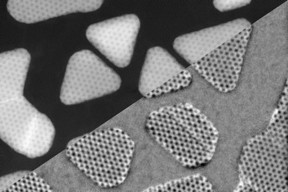 |
| These images of "islands" of gold atoms deposited on a layer of two-dimensional molybdenum sulfide were produced by two different modes, using a new scanning tunneling electron microscope (STEM) in the new MIT.nano facility. By combining the data from the two different modes the researchers were able to figure out the three-dimensional arrangement of atoms where the two materials meet. Credits:Image courtesy of the researchers |
Abstract:
In recent years, engineers have found ways to modify the properties of some “two- dimensional” materials, which are just one or a few atoms thick, by stacking two layers together and rotating one slightly in relation to the other. This creates what are known as moiré patterns, where tiny shifts in the alignment of atoms between the two sheets create larger-scale patterns. It also changes the way electrons move through the material, in potentially useful ways.
Engineering the boundary between 2D and 3D materials: Cutting-edge microscope helps reveal ways to control the electronic properties of atomically thin materials
Cambridge, MA | Posted on February 26th, 2021But for practical applications, such two-dimensional materials must at some point connect with the ordinary world of 3D materials. An international team led by MIT researchers has now come up with a way of imaging what goes on at these interfaces, down to the level of individual atoms, and of correlating the moiré patterns at the 2D-3D boundary with the resulting changes in the material’s properties.
The new findings are described today in the journal Nature Communications, in a paper by MIT graduate students Kate Reidy and Georgios Varnavides, professors of materials science and engineering Frances Ross, Jim LeBeau, and Polina Anikeeva, and five others at MIT, Harvard University, and the University of Victoria in Canada.
Pairs of two-dimensional materials such as graphene or hexagonal boron nitride can exhibit amazing variations in their behavior when the two sheets are just slightly twisted relative to each other. That causes the chicken-wire-like atomic lattices to form moiré patterns, the kinds of odd bands and blobs that sometimes appear when taking a picture of a printed image, or through a window screen. In the case of 2D materials, “it seems like anything, every interesting materials property you can think of, you can somehow modulate or change by twisting the 2D materials with respect to each other,” says Ross, who is the Ellen Swallow Richards Professor at MIT.
While these 2D pairings have attracted scientific attention worldwide, she says, little has been known about what happens where 2D materials meet regular 3D solids. “What got us interested in this topic,” Ross says, was “what happens when a 2D material and a 3D material are put together. Firstly, how do you measure the atomic positions at, and near, the interface? Secondly, what are the differences between a 3D-2D and a 2D-2D interface? And thirdly, how you might control it — is there a way to deliberately design the interfacial structure” to produce desired properties?
Figuring out exactly what happens at such 2D-3D interfaces was a daunting challenge because electron microscopes produce an image of the sample in projection, and they’re limited in their ability to extract depth information needed to analyze details of the interface structure. But the team figured out a set of algorithms that allowed them to extrapolate back from images of the sample, which look somewhat like a set of overlapping shadows, to figure out which configuration of stacked layers would yield that complex “shadow.”
The team made use of two unique transmission electron microscopes at MIT that enable a combination of capabilities that is unrivalled in the world. In one of these instruments, a microscope is connected directly to a fabrication system so that samples can be produced onsite by deposition processes and immediately fed straight into the imaging system. This is one of only a few such facilities worldwide, which use an ultrahigh vacuum system that prevents even the tiniest of impurities from contaminating the sample as the 2D-3D interface is being prepared. The second instrument is a scanning transmission electron microscope located in MIT’s new research facility, MIT.nano. This microscope has outstanding stability for high-resolution imaging, as well as multiple imaging modes for collecting information about the sample.
Unlike stacked 2D materials, whose orientations can be relatively easily changed by simply picking up one layer, twisting it slightly, and placing it down again, the bonds holding 3D materials together are much stronger, so the team had to develop new ways of obtaining aligned layers. To do this, they added the 3D material onto the 2D material in ultrahigh vacuum, choosing growth conditions where the layers self-assembled in a reproducible orientation with specific degrees of twist. “We had to grow a structure that was going to be aligned in a certain way,” Reidy says.
Having grown the materials, they then had to figure out how to reveal the atomic configurations and orientations of the different layers. A scanning transmission electron microscope actually produces more information than is apparent in a flat image; in fact, every point in the image contains details of the paths along which the electrons arrived and departed (the process of diffraction), as well as any energy that the electrons lost in the process. All these data can be separated out so that the information at all points in an image can be used to decode the actual solid structure. This process is only possible for state-of-the-art microscopes, such as that in MIT.nano, which generates a probe of electrons that is unusually narrow and precise.
The researchers used a combination of techniques called 4D STEM and integrated differential phase contrast to achieve that process of extracting the full structure at the interface from the image. Then, Varnavides says, they asked, “Now that we can image the full structure at the interface, what does this mean for our understanding of the properties of this interface?” The researchers showed through modeling that electronic properties are expected to be modified in a way that can only be understood if the full structure of the interface is included in the physical theory. “What we found is that indeed this stacking, the way the atoms are stacked out-of-plane, does modulate the electronic and charge density properties,” he says.
Ross says the findings could help lead to improved kinds of junctions in some microchips, for example. “Every 2D material that’s used in a device has to exist in the 3D world, and so it has to have a junction somehow with three-dimensional materials,” she says. So, with this better understanding of those interfaces, and new ways to study them in action, “we’re in good shape for making structures with desirable properties in a kind of planned rather than ad hoc way.”
“The methodology used has the potential to calculate from the acquired local diffraction patterns the modulation of the local electron momentum,” he says, adding that “the methodology and research shown here has an outstanding future and high interest for the materials science community.”
###
Written by David L. Chandler, MIT News Office
####
For more information, please click here
Contacts:
Abby Abazorius
MIT News Office
617.253.2709
Copyright © Massachusetts Institute of Technology
If you have a comment, please Contact us.Issuers of news releases, not 7th Wave, Inc. or Nanotechnology Now, are solely responsible for the accuracy of the content.
Bookmark:


| Related Links |
| Related News Press |
News and information
![]() Simulating magnetization in a Heisenberg quantum spin chain April 5th, 2024
Simulating magnetization in a Heisenberg quantum spin chain April 5th, 2024
![]() NRL charters Navy’s quantum inertial navigation path to reduce drift April 5th, 2024
NRL charters Navy’s quantum inertial navigation path to reduce drift April 5th, 2024
![]() Discovery points path to flash-like memory for storing qubits: Rice find could hasten development of nonvolatile quantum memory April 5th, 2024
Discovery points path to flash-like memory for storing qubits: Rice find could hasten development of nonvolatile quantum memory April 5th, 2024
Imaging
![]() Nanoscale CL thermometry with lanthanide-doped heavy-metal oxide in TEM March 8th, 2024
Nanoscale CL thermometry with lanthanide-doped heavy-metal oxide in TEM March 8th, 2024
2 Dimensional Materials
![]() NRL discovers two-dimensional waveguides February 16th, 2024
NRL discovers two-dimensional waveguides February 16th, 2024
Graphene/ Graphite
![]() NRL discovers two-dimensional waveguides February 16th, 2024
NRL discovers two-dimensional waveguides February 16th, 2024
Possible Futures
![]() Discovery points path to flash-like memory for storing qubits: Rice find could hasten development of nonvolatile quantum memory April 5th, 2024
Discovery points path to flash-like memory for storing qubits: Rice find could hasten development of nonvolatile quantum memory April 5th, 2024
![]() With VECSELs towards the quantum internet Fraunhofer: IAF achieves record output power with VECSEL for quantum frequency converters April 5th, 2024
With VECSELs towards the quantum internet Fraunhofer: IAF achieves record output power with VECSEL for quantum frequency converters April 5th, 2024
Chip Technology
![]() Discovery points path to flash-like memory for storing qubits: Rice find could hasten development of nonvolatile quantum memory April 5th, 2024
Discovery points path to flash-like memory for storing qubits: Rice find could hasten development of nonvolatile quantum memory April 5th, 2024
![]() Utilizing palladium for addressing contact issues of buried oxide thin film transistors April 5th, 2024
Utilizing palladium for addressing contact issues of buried oxide thin film transistors April 5th, 2024
![]() HKUST researchers develop new integration technique for efficient coupling of III-V and silicon February 16th, 2024
HKUST researchers develop new integration technique for efficient coupling of III-V and silicon February 16th, 2024
Nanoelectronics
![]() Interdisciplinary: Rice team tackles the future of semiconductors Multiferroics could be the key to ultralow-energy computing October 6th, 2023
Interdisciplinary: Rice team tackles the future of semiconductors Multiferroics could be the key to ultralow-energy computing October 6th, 2023
![]() Key element for a scalable quantum computer: Physicists from Forschungszentrum Jülich and RWTH Aachen University demonstrate electron transport on a quantum chip September 23rd, 2022
Key element for a scalable quantum computer: Physicists from Forschungszentrum Jülich and RWTH Aachen University demonstrate electron transport on a quantum chip September 23rd, 2022
![]() Reduced power consumption in semiconductor devices September 23rd, 2022
Reduced power consumption in semiconductor devices September 23rd, 2022
![]() Atomic level deposition to extend Moore’s law and beyond July 15th, 2022
Atomic level deposition to extend Moore’s law and beyond July 15th, 2022
Discoveries
![]() Chemical reactions can scramble quantum information as well as black holes April 5th, 2024
Chemical reactions can scramble quantum information as well as black holes April 5th, 2024
![]() New micromaterial releases nanoparticles that selectively destroy cancer cells April 5th, 2024
New micromaterial releases nanoparticles that selectively destroy cancer cells April 5th, 2024
![]() Utilizing palladium for addressing contact issues of buried oxide thin film transistors April 5th, 2024
Utilizing palladium for addressing contact issues of buried oxide thin film transistors April 5th, 2024
Announcements
![]() NRL charters Navy’s quantum inertial navigation path to reduce drift April 5th, 2024
NRL charters Navy’s quantum inertial navigation path to reduce drift April 5th, 2024
![]() Discovery points path to flash-like memory for storing qubits: Rice find could hasten development of nonvolatile quantum memory April 5th, 2024
Discovery points path to flash-like memory for storing qubits: Rice find could hasten development of nonvolatile quantum memory April 5th, 2024
Interviews/Book Reviews/Essays/Reports/Podcasts/Journals/White papers/Posters
![]() Simulating magnetization in a Heisenberg quantum spin chain April 5th, 2024
Simulating magnetization in a Heisenberg quantum spin chain April 5th, 2024
![]() Discovery points path to flash-like memory for storing qubits: Rice find could hasten development of nonvolatile quantum memory April 5th, 2024
Discovery points path to flash-like memory for storing qubits: Rice find could hasten development of nonvolatile quantum memory April 5th, 2024
Tools
![]() Ferroelectrically modulate the Fermi level of graphene oxide to enhance SERS response November 3rd, 2023
Ferroelectrically modulate the Fermi level of graphene oxide to enhance SERS response November 3rd, 2023
![]() The USTC realizes In situ electron paramagnetic resonance spectroscopy using single nanodiamond sensors November 3rd, 2023
The USTC realizes In situ electron paramagnetic resonance spectroscopy using single nanodiamond sensors November 3rd, 2023
|
|
||
|
|
||
| The latest news from around the world, FREE | ||
|
|
||
|
|
||
| Premium Products | ||
|
|
||
|
Only the news you want to read!
Learn More |
||
|
|
||
|
Full-service, expert consulting
Learn More |
||
|
|
||