Home > Press > 2D crystals conforming to 3D curves create strain for engineering quantum devices
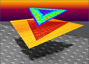 |
| Strain-tolerant, triangular, monolayer crystals of WS2 were grown on SiO2 substrates patterned with donut-shaped pillars, as shown in scanning electron microscope (bottom) and atomic force microscope (middle) image elements. The curvature of the pillars induced strain in the overlying crystals that locally altered their optoelectronic properties, as shown in bright regions of photoluminescence (top). CREDIT Christopher Rouleau/Oak Ridge National Laboratory, US Dept. of Energy |
Abstract:
A team led by scientists at the Department of Energy's Oak Ridge National Laboratory explored how atomically thin two-dimensional (2D) crystals can grow over 3D objects and how the curvature of those objects can stretch and strain the crystals. The findings, published in Science Advances, point to a strategy for engineering strain directly during the growth of atomically thin crystals to fabricate single photon emitters for quantum information processing.
2D crystals conforming to 3D curves create strain for engineering quantum devices
Oak Ridge, TN | Posted on June 7th, 2019The team first explored growth of the flat crystals on substrates patterned with sharp steps and trenches. Surprisingly, the crystals conformally grew up and down these flat obstacles without changing their properties or growth rates. However, curvy surfaces required the crystals to stretch as they grew to maintain their crystal structure. This growth of 2D crystals into the third dimension presented a fascinating opportunity.
"You can engineer how much strain you impart to a crystal by designing objects for them to grow over," said Kai Xiao, who with ORNL colleagues David Geohegan and postdoctoral researcher Kai Wang (now at Intel) conceived the study. "Strain is one way to make 'hot spots' for single photon emitters."
Conformal growth of perfect 2D crystals over 3D objects has the promise to localize strain to create high-fidelity arrays of single photon emitters. Stretching or compressing the crystal lattice changes the material's band gap, the energy gap between the valence and conduction bands of electrons, which largely determines a material's optoelectronic properties. Using strain engineering, researchers can funnel charge carriers to recombine precisely where desired in the crystal instead of at random defect locations. By tailoring curved objects to localize strain in the crystal, and then measuring resulting shifts in optical properties, the experimentalists compelled co-authors at Rice University--theorists Henry Yu, Nitant Gupta and Boris Yakobson--to simulate and map how curvature induces strain during crystal growth.
At ORNL, Wang and Xiao designed experiments with Bernadeta Srijanto to explore the growth of 2D crystals over lithographically patterned arrays of nanoscale shapes. Srijanto first used photolithography masks to protect certain areas of a silicon oxide surface during exposure to light, and then etched away the exposed surfaces to leave vertically standing shapes, including donuts, cones and steps. Wang and another postdoctoral researcher, Xufan Li (now at Honda Research Institute), then inserted the substrates into a furnace where vaporized tungsten oxide and sulfur reacted to deposit tungsten disulfide on the substrates as monolayer crystals. The crystals grew as an orderly lattice of atoms in perfect triangular tiles that grew larger with time by adding row after row of atoms to their outer edges. While the 2D crystals seemed to effortlessly fold like paper over tall steps and sharp trenches, growth over curved objects forced the crystals to stretch to maintain their triangular shape.
The scientists found that "donuts" 40 nanometers high were great candidates for single photon emitters because the crystals could reliably tolerate the strain they induced, and the maximum strain was precisely in the "hole" of the donut, as measured by shifts in the photoluminescence and Raman scattering. In the future, arrays of donuts or other structures could be patterned anywhere that quantum emitters are desired before the crystals are grown.
Wang and ORNL co-author Alex Puretzky used photoluminescence mapping to reveal where the crystals nucleated and how fast each edge of the triangular crystal progressed as it grew over the donuts. After careful analysis of the images, they were surprised to discover that although the crystals maintained their perfect shapes, the edges of crystals that had been strained by donuts grew faster.
To explain this acceleration, Puretzky developed a crystal growth model, and colleague Mina Yoon conducted first-principles calculations. Their work showed that strain is more likely to induce defects on the growing edge of a crystal. These defects can multiply the number of nucleation sites that seed crystal growth along an edge, allowing it to grow faster than before.
The reason crystals can grow easily up and down deep trenches, but become strained by shallow donuts, has to do with conformity and curvature. Imagine wrapping presents. Boxes are easy to wrap because the paper can fold to conform to the shape. But an irregularly shaped object with curves, such as an unboxed mug, is impossible to wrap conformally (to avoid tearing the paper, you would have to be able to stretch it like plastic wrap.)
The 2D crystals also stretch to conform to the substrate's curves. Eventually, however, the strain becomes too great and the crystals split to release the strain, atomic force microscopy and other techniques revealed. After the crystal cracks, growth of the still-strained material proceeds in different directions for each new arm. At Nanjing University of Aeronautics and Astronautics, Zhili Hu performed phase-field simulations of crystal branching. Xiang Gao of ORNL and Mengkun Tian (formerly of the University of Tennessee) analyzed the atomic structure of the crystals by scanning transmission electron microscopy.
"The results present exciting opportunities to take two-dimensional materials and vertically integrate them into the third dimension for next-generation electronics," said Xiao.
Next the researchers will explore whether strain can enhance the performance of tailored materials. "We're exploring how the strain of the crystal can make it easier to induce a phase change so the crystal can take on entirely new properties," Xiao said. "At the Center for Nanophase Materials Sciences, we're developing tools that will allow us to probe these structures and their quantum information aspects."
###
The title of the paper is "Strain tolerance of two-dimensional crystal growth on curved surfaces."
####
For more information, please click here
Contacts:
Dawn Levy
865-576-6448
Copyright © Oak Ridge National Laboratory
If you have a comment, please Contact us.Issuers of news releases, not 7th Wave, Inc. or Nanotechnology Now, are solely responsible for the accuracy of the content.
Bookmark:


| Related News Press |
News and information
![]() Simulating magnetization in a Heisenberg quantum spin chain April 5th, 2024
Simulating magnetization in a Heisenberg quantum spin chain April 5th, 2024
![]() NRL charters Navy�s quantum inertial navigation path to reduce drift April 5th, 2024
NRL charters Navy�s quantum inertial navigation path to reduce drift April 5th, 2024
![]() Discovery points path to flash-like memory for storing qubits: Rice find could hasten development of nonvolatile quantum memory April 5th, 2024
Discovery points path to flash-like memory for storing qubits: Rice find could hasten development of nonvolatile quantum memory April 5th, 2024
Imaging
![]() Nanoscale CL thermometry with lanthanide-doped heavy-metal oxide in TEM March 8th, 2024
Nanoscale CL thermometry with lanthanide-doped heavy-metal oxide in TEM March 8th, 2024
2 Dimensional Materials
![]() NRL discovers two-dimensional waveguides February 16th, 2024
NRL discovers two-dimensional waveguides February 16th, 2024
Nanofabrication
![]() New chip opens door to AI computing at light speed February 16th, 2024
New chip opens door to AI computing at light speed February 16th, 2024
Laboratories
![]() A battery�s hopping ions remember where they�ve been: Seen in atomic detail, the seemingly smooth flow of ions through a battery�s electrolyte is surprisingly complicated February 16th, 2024
A battery�s hopping ions remember where they�ve been: Seen in atomic detail, the seemingly smooth flow of ions through a battery�s electrolyte is surprisingly complicated February 16th, 2024
![]() NRL discovers two-dimensional waveguides February 16th, 2024
NRL discovers two-dimensional waveguides February 16th, 2024
Govt.-Legislation/Regulation/Funding/Policy
![]() NRL charters Navy�s quantum inertial navigation path to reduce drift April 5th, 2024
NRL charters Navy�s quantum inertial navigation path to reduce drift April 5th, 2024
![]() Discovery points path to flash-like memory for storing qubits: Rice find could hasten development of nonvolatile quantum memory April 5th, 2024
Discovery points path to flash-like memory for storing qubits: Rice find could hasten development of nonvolatile quantum memory April 5th, 2024
![]() Chemical reactions can scramble quantum information as well as black holes April 5th, 2024
Chemical reactions can scramble quantum information as well as black holes April 5th, 2024
Possible Futures
![]() Discovery points path to flash-like memory for storing qubits: Rice find could hasten development of nonvolatile quantum memory April 5th, 2024
Discovery points path to flash-like memory for storing qubits: Rice find could hasten development of nonvolatile quantum memory April 5th, 2024
![]() With VECSELs towards the quantum internet Fraunhofer: IAF achieves record output power with VECSEL for quantum frequency converters April 5th, 2024
With VECSELs towards the quantum internet Fraunhofer: IAF achieves record output power with VECSEL for quantum frequency converters April 5th, 2024
Discoveries
![]() Chemical reactions can scramble quantum information as well as black holes April 5th, 2024
Chemical reactions can scramble quantum information as well as black holes April 5th, 2024
![]() New micromaterial releases nanoparticles that selectively destroy cancer cells April 5th, 2024
New micromaterial releases nanoparticles that selectively destroy cancer cells April 5th, 2024
![]() Utilizing palladium for addressing contact issues of buried oxide thin film transistors April 5th, 2024
Utilizing palladium for addressing contact issues of buried oxide thin film transistors April 5th, 2024
Interviews/Book Reviews/Essays/Reports/Podcasts/Journals/White papers/Posters
![]() Simulating magnetization in a Heisenberg quantum spin chain April 5th, 2024
Simulating magnetization in a Heisenberg quantum spin chain April 5th, 2024
![]() Discovery points path to flash-like memory for storing qubits: Rice find could hasten development of nonvolatile quantum memory April 5th, 2024
Discovery points path to flash-like memory for storing qubits: Rice find could hasten development of nonvolatile quantum memory April 5th, 2024
Tools
![]() Ferroelectrically modulate the Fermi level of graphene oxide to enhance SERS response November 3rd, 2023
Ferroelectrically modulate the Fermi level of graphene oxide to enhance SERS response November 3rd, 2023
![]() The USTC realizes In situ electron paramagnetic resonance spectroscopy using single nanodiamond sensors November 3rd, 2023
The USTC realizes In situ electron paramagnetic resonance spectroscopy using single nanodiamond sensors November 3rd, 2023
Research partnerships
![]() Discovery points path to flash-like memory for storing qubits: Rice find could hasten development of nonvolatile quantum memory April 5th, 2024
Discovery points path to flash-like memory for storing qubits: Rice find could hasten development of nonvolatile quantum memory April 5th, 2024
![]() Researchers� approach may protect quantum computers from attacks March 8th, 2024
Researchers� approach may protect quantum computers from attacks March 8th, 2024
![]() 'Sudden death' of quantum fluctuations defies current theories of superconductivity: Study challenges the conventional wisdom of superconducting quantum transitions January 12th, 2024
'Sudden death' of quantum fluctuations defies current theories of superconductivity: Study challenges the conventional wisdom of superconducting quantum transitions January 12th, 2024
Quantum nanoscience
![]() Simulating magnetization in a Heisenberg quantum spin chain April 5th, 2024
Simulating magnetization in a Heisenberg quantum spin chain April 5th, 2024
![]() Optically trapped quantum droplets of light can bind together to form macroscopic complexes March 8th, 2024
Optically trapped quantum droplets of light can bind together to form macroscopic complexes March 8th, 2024
![]() Bridging light and electrons January 12th, 2024
Bridging light and electrons January 12th, 2024
![]() 'Sudden death' of quantum fluctuations defies current theories of superconductivity: Study challenges the conventional wisdom of superconducting quantum transitions January 12th, 2024
'Sudden death' of quantum fluctuations defies current theories of superconductivity: Study challenges the conventional wisdom of superconducting quantum transitions January 12th, 2024
|
|
||
|
|
||
| The latest news from around the world, FREE | ||
|
|
||
|
|
||
| Premium Products | ||
|
|
||
|
Only the news you want to read!
Learn More |
||
|
|
||
|
Full-service, expert consulting
Learn More |
||
|
|
||