Home > Press > Leti Integrates Hybrid III-V Silicon Lasers on 200mm Wafers with Standard CMOS Process
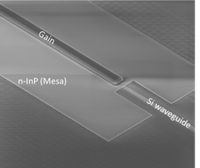 |
| Tilted scanning electron microscopy view of the III-V/Si DFB laser after the IIIV patterning steps. |
Abstract:
Leti, a research institute of CEA Tech, has integrated hybrid III-V silicon lasers on 200mm wafers using standard CMOS process flow. This breakthrough shows the way to transitioning away from 100mm wafers and a process based on bulk III-V technology that requires contacts with noble metals and lift-off based patterning.
Leti Integrates Hybrid III-V Silicon Lasers on 200mm Wafers with Standard CMOS Process
San Francisco, CA | Posted on December 6th, 2017The project, carried out in the framework of the IRT Nanoelec program, which is headed by Leti, demonstrated that the hybrid device�s performance is comparable to the reference device fabricated with the current process on 100mm wafers. The fabrication flow is fully planar and compatible with large-scale integration on silicon-photonic circuits.
The results were reported Dec. 5 at IEDM 2017 in a paper titled �Hybrid III-V/Si DFB Laser Integration on a 200mm Fully CMOS-compatible Silicon Photonics Platform�.
CMOS compatibility with silicon photonics lowers fabrication costs, and provides access to mature and large-scale facilities, which enables packaging compatibility with CMOS driving circuits.
�Silicon-photonic technologies are becoming more mature, but the main limitation of these platforms is the lack of an integrated light source,� said Bertrand Szelag, a co-author of the paper. �This project showed that a laser can be integrated on a mature silicon-photonic platform with a modular approach that does not compromise baseline process performances. We demonstrated that the entire process can be done in a standard CMOS fabrication line with conventional process and materials, and that it is possible to integrate all the photonic building blocks at large scale.�
The integration required managing a thick silicon film, typically 500nm thick, for the hybrid laser, and a thinner one, typically 300nm, for the baseline silicon-photonic platform. This required locally thickening the silicon by adding 200nm of amorphous silicon via a damascene process, which presents the advantage of leaving a flat surface favorable for bonding III-V silicon. The laser can be integrated on a mature silicon photonic platform with a modular approach that does not compromise the baseline process performance.
The novelty of the approach also included using innovative laser electrical contacts that do not contain any noble metals, such as gold. The contacts also prohibit integration lift-off-based processes. Nickel-based metallization was used with an integration technique similar to a CMOS transistor technique, in which tungsten plugs connect the device to the routing metal lines.
Next steps include integrating the laser with active silicon-photonic devices, e.g. a modulator and photodiode with several interconnect metal levels in a planarized backend. Finally, III-V die bonding will replace III-V wafer bonding in order to process lasers on the entire silicon wafer.
####
About Leti
Leti, a technology research institute at CEA Tech, is a global leader in miniaturization technologies enabling smart, energy-efficient and secure solutions for industry. Founded in 1967, Leti pioneers micro-& nanotechnologies, tailoring differentiating applicative solutions for global companies, SMEs and startups. Leti tackles critical challenges in healthcare, energy and digital migration. From sensors to data processing and computing solutions, Leti�s multidisciplinary teams deliver solid expertise, leveraging world-class pre-industrialization facilities. With a staff of more than 1,900, a portfolio of 2,700 patents, 91,500 sq. ft. of cleanroom space and a clear IP policy, the institute is based in Grenoble, France, and has offices in Silicon Valley and Tokyo. Leti has launched 60 startups and is a member of the Carnot Institutes network. This year, the institute celebrates its 50th anniversary. Follow us on www.leti-cea.com and @CEA_Leti.
CEA Tech is the technology research branch of the French Alternative Energies and Atomic Energy Commission (CEA), a key player in innovative R&D, defence & security, nuclear energy, technological research for industry and fundamental science, identified by Thomson Reuters as the second most innovative research organization in the world. CEA Tech leverages a unique innovation-driven culture and unrivalled expertise to develop and disseminate new technologies for industry, helping to create high-end products and provide a competitive edge.
For more information, please click here
Contacts:
Press Contact
Agency
+33 6 74 93 23 47
Copyright © Leti
If you have a comment, please Contact us.Issuers of news releases, not 7th Wave, Inc. or Nanotechnology Now, are solely responsible for the accuracy of the content.
Bookmark:


| Related News Press |
News and information
![]() Simulating magnetization in a Heisenberg quantum spin chain April 5th, 2024
Simulating magnetization in a Heisenberg quantum spin chain April 5th, 2024
![]() NRL charters Navy�s quantum inertial navigation path to reduce drift April 5th, 2024
NRL charters Navy�s quantum inertial navigation path to reduce drift April 5th, 2024
![]() Discovery points path to flash-like memory for storing qubits: Rice find could hasten development of nonvolatile quantum memory April 5th, 2024
Discovery points path to flash-like memory for storing qubits: Rice find could hasten development of nonvolatile quantum memory April 5th, 2024
Hardware
![]() The present and future of computing get a boost from new research July 21st, 2023
The present and future of computing get a boost from new research July 21st, 2023
![]() A Carbon Nanotube Microprocessor Mature Enough to Say Hello: Three new breakthroughs make commercial nanotube processors possible March 2nd, 2020
A Carbon Nanotube Microprocessor Mature Enough to Say Hello: Three new breakthroughs make commercial nanotube processors possible March 2nd, 2020
![]() Powering the future: Smallest all-digital circuit opens doors to 5 nm next-gen semiconductor February 11th, 2020
Powering the future: Smallest all-digital circuit opens doors to 5 nm next-gen semiconductor February 11th, 2020
Possible Futures
![]() Discovery points path to flash-like memory for storing qubits: Rice find could hasten development of nonvolatile quantum memory April 5th, 2024
Discovery points path to flash-like memory for storing qubits: Rice find could hasten development of nonvolatile quantum memory April 5th, 2024
![]() With VECSELs towards the quantum internet Fraunhofer: IAF achieves record output power with VECSEL for quantum frequency converters April 5th, 2024
With VECSELs towards the quantum internet Fraunhofer: IAF achieves record output power with VECSEL for quantum frequency converters April 5th, 2024
Chip Technology
![]() Discovery points path to flash-like memory for storing qubits: Rice find could hasten development of nonvolatile quantum memory April 5th, 2024
Discovery points path to flash-like memory for storing qubits: Rice find could hasten development of nonvolatile quantum memory April 5th, 2024
![]() Utilizing palladium for addressing contact issues of buried oxide thin film transistors April 5th, 2024
Utilizing palladium for addressing contact issues of buried oxide thin film transistors April 5th, 2024
![]() HKUST researchers develop new integration technique for efficient coupling of III-V and silicon February 16th, 2024
HKUST researchers develop new integration technique for efficient coupling of III-V and silicon February 16th, 2024
Discoveries
![]() Chemical reactions can scramble quantum information as well as black holes April 5th, 2024
Chemical reactions can scramble quantum information as well as black holes April 5th, 2024
![]() New micromaterial releases nanoparticles that selectively destroy cancer cells April 5th, 2024
New micromaterial releases nanoparticles that selectively destroy cancer cells April 5th, 2024
![]() Utilizing palladium for addressing contact issues of buried oxide thin film transistors April 5th, 2024
Utilizing palladium for addressing contact issues of buried oxide thin film transistors April 5th, 2024
Announcements
![]() NRL charters Navy�s quantum inertial navigation path to reduce drift April 5th, 2024
NRL charters Navy�s quantum inertial navigation path to reduce drift April 5th, 2024
![]() Discovery points path to flash-like memory for storing qubits: Rice find could hasten development of nonvolatile quantum memory April 5th, 2024
Discovery points path to flash-like memory for storing qubits: Rice find could hasten development of nonvolatile quantum memory April 5th, 2024
Photonics/Optics/Lasers
![]() With VECSELs towards the quantum internet Fraunhofer: IAF achieves record output power with VECSEL for quantum frequency converters April 5th, 2024
With VECSELs towards the quantum internet Fraunhofer: IAF achieves record output power with VECSEL for quantum frequency converters April 5th, 2024
![]() Nanoscale CL thermometry with lanthanide-doped heavy-metal oxide in TEM March 8th, 2024
Nanoscale CL thermometry with lanthanide-doped heavy-metal oxide in TEM March 8th, 2024
![]() Optically trapped quantum droplets of light can bind together to form macroscopic complexes March 8th, 2024
Optically trapped quantum droplets of light can bind together to form macroscopic complexes March 8th, 2024
![]() HKUST researchers develop new integration technique for efficient coupling of III-V and silicon February 16th, 2024
HKUST researchers develop new integration technique for efficient coupling of III-V and silicon February 16th, 2024
|
|
||
|
|
||
| The latest news from around the world, FREE | ||
|
|
||
|
|
||
| Premium Products | ||
|
|
||
|
Only the news you want to read!
Learn More |
||
|
|
||
|
Full-service, expert consulting
Learn More |
||
|
|
||