Home > Press > Scientists have shown how to make a low-cost yet high precision glass nanoengraving: In a joint study, scientists have developed a mechanism of laser deposition of patterns on glass with a resolution of 1000 times lower than the width of a human hair
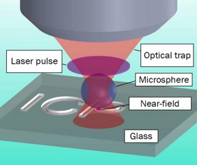 |
| This is a picture of the experimental setup. CREDIT: ACS Publications/Applied Materials & Interfaces |
Abstract:
In a joint study, scientists from the MIPT (Moscow Institute of Physics and Technology), ICP (Institute of Chemical Physics) named after Semenov, MSU (Moscow State University) and IPCP (Institute of Problems of Chemical Physics) have developed a mechanism of laser deposition of patterns on glass with a resolution of 1000 times lower than the width of a human hair. Focusing the laser was conducted with the help of small glass spheres, playing the role of the lens. This mechanism allows inexpensively and relatively easy to apply complex patterns to a glass surface, whereby obtaining a spatial resolution of less than 100 nanometers.
Scientists have shown how to make a low-cost yet high precision glass nanoengraving: In a joint study, scientists have developed a mechanism of laser deposition of patterns on glass with a resolution of 1000 times lower than the width of a human hair
Moscow, Russia | Posted on January 21st, 2016The proposed method will allow sufficiently quick and cheap creation of sensors and microchips of a nanoscale. According to the scientists, it is much cheaper and technologically easier than any of previously used methods, in addition to the fact that the new application allows deposition of the computer drawings on the glass surface with an acceptable resolution. To demonstrate this method, the abbreviation of the Institute of Chemical Physics (ICP) was deposited on glass with a high resolution (about 100 nanometers). In particular, nanoengraving is used to create ultra-precise circuits in microfluidics. The operating fluid can flow through the engraved channels connecting various parts of the circuit; and the smaller the size of such a circuit, the higher the engraving resolution.
A femtosecond laser used by scientists allows deposition of complex two-and three-dimensional patterns on the surface of transparent materials. Resolution -- the minimum size of the pattern's image detail -- is always a problem in these kinds of tasks, since it is limited (for physical reasons) by the laser wavelength. The higher the resolution, the smaller the size of patterns applied and the more interesting and sought-after these patterns in technology.
To improve the resolution, the near-field effect is often used. This method involves focusing a laser beam, using metal nanoparticles or a layer of dielectric microspheres as "lens". However, these methods complicate the pattern's deposition process, as the "lens" are fixed in space.
In their work, the authors propose a different approach: using a beam of light in fluid, they create a kind of a trap where they place glass microspheres. The advantage of this focusing method consists in that, that the "trap" can be moved, thereby moving the "lens" in space and focusing the laser to the desired area of the glass.
However, simply moving a laser beam along the surface is not enough. Exposure to laser leads to the formation of hillocks but not craters. These hillocks are quite rough and wide, but the effect of alkali at a temperature of 90� C turns the hillocks into smooth craters with a smaller width. Whereas such a two-step structuring allows achievement of a resolution below 100 nanometers (nm), one-step structuring, when the surface is treated only with a laser, does not allow obtaining precision below 150-200 nm (depending on the complexity of the structure).
As a result, the whole process of nanoengraving appears as follows. Initially, the glass surface is irradiated with a femtosecond laser. The laser pulse is focused by means of a glass bead, which is guided by an optical "trap" to a predetermined area of the glass. As a result, wide hillocks are formed on the surface of glass; but then, after surface treatment with an alkaline solution, these hillocks are converted to smaller craters of more streamlined shapes.
In addition to direct patterning process, the scientists investigated dependence of the resolution, i.e. the crater size, from the laser power. The results showed that for obtaining greater precision, it will be more effective to use small spheres, which allow obtaining a resolution below 100 nm.
The minimum width of the crater obtained was 70 nm. The figure below shows this particular crater, and the chart shows the shape of the crater on two axes.
For practical use of this method -- in addition to high resolution, you must also take into account the complexity of applying intricate structures. The above publication shows that if you use the engraving technique described, you will be able to apply relatively complex structures. To prove this, the glass surface was engraved with the abbreviation for the Institute of Chemical Physics (ICP). The average width of each letter is 100 nm, depth -- 20 nm (see Fig. below with a scale - 500 nm).
"Creating thin grooves and channels can be used in chemistry and biology fields - in the production of 'microfluidics' and at various 'nano-plants'," -- says Aleksander Shakhov, the article's co-author, post-graduate of the Faculty of General and Applied Physics at MIPT. "Channels" for liquids engraved by methods described above are used for the development of small precise sensors working with liquids. The article in question also suggests a sufficiently fast and cheap mechanism for nanostructuring. Such an approach, in particular, can allow rapid and technologically uncomplicated creation of inexpensive devices and sensors by applying complex structures of thin grooves and channels through which operating fluid will flow.
####
For more information, please click here
Contacts:
Valerii Roizen
7-929-992-2721
Copyright © Moscow Institute of Physics and Technology
If you have a comment, please Contact us.Issuers of news releases, not 7th Wave, Inc. or Nanotechnology Now, are solely responsible for the accuracy of the content.
Bookmark:


| Related Links |
| Related News Press |
News and information
![]() Simulating magnetization in a Heisenberg quantum spin chain April 5th, 2024
Simulating magnetization in a Heisenberg quantum spin chain April 5th, 2024
![]() NRL charters Navy�s quantum inertial navigation path to reduce drift April 5th, 2024
NRL charters Navy�s quantum inertial navigation path to reduce drift April 5th, 2024
![]() Discovery points path to flash-like memory for storing qubits: Rice find could hasten development of nonvolatile quantum memory April 5th, 2024
Discovery points path to flash-like memory for storing qubits: Rice find could hasten development of nonvolatile quantum memory April 5th, 2024
Chemistry
![]() What heat can tell us about battery chemistry: using the Peltier effect to study lithium-ion cells March 8th, 2024
What heat can tell us about battery chemistry: using the Peltier effect to study lithium-ion cells March 8th, 2024
![]() Nanoscale CL thermometry with lanthanide-doped heavy-metal oxide in TEM March 8th, 2024
Nanoscale CL thermometry with lanthanide-doped heavy-metal oxide in TEM March 8th, 2024
Microfluidics/Nanofluidics
![]() Implantable device shrinks pancreatic tumors: Taming pancreatic cancer with intratumoral immunotherapy April 14th, 2023
Implantable device shrinks pancreatic tumors: Taming pancreatic cancer with intratumoral immunotherapy April 14th, 2023
![]() Researchers design new inks for 3D-printable wearable bioelectronics: Potential uses include printing electronic tattoos for medical tracking applications August 19th, 2022
Researchers design new inks for 3D-printable wearable bioelectronics: Potential uses include printing electronic tattoos for medical tracking applications August 19th, 2022
![]() Oregon State University research pushes closer to new therapy for pancreatic cancer May 6th, 2022
Oregon State University research pushes closer to new therapy for pancreatic cancer May 6th, 2022
Possible Futures
![]() Discovery points path to flash-like memory for storing qubits: Rice find could hasten development of nonvolatile quantum memory April 5th, 2024
Discovery points path to flash-like memory for storing qubits: Rice find could hasten development of nonvolatile quantum memory April 5th, 2024
![]() With VECSELs towards the quantum internet Fraunhofer: IAF achieves record output power with VECSEL for quantum frequency converters April 5th, 2024
With VECSELs towards the quantum internet Fraunhofer: IAF achieves record output power with VECSEL for quantum frequency converters April 5th, 2024
Chip Technology
![]() Discovery points path to flash-like memory for storing qubits: Rice find could hasten development of nonvolatile quantum memory April 5th, 2024
Discovery points path to flash-like memory for storing qubits: Rice find could hasten development of nonvolatile quantum memory April 5th, 2024
![]() Utilizing palladium for addressing contact issues of buried oxide thin film transistors April 5th, 2024
Utilizing palladium for addressing contact issues of buried oxide thin film transistors April 5th, 2024
![]() HKUST researchers develop new integration technique for efficient coupling of III-V and silicon February 16th, 2024
HKUST researchers develop new integration technique for efficient coupling of III-V and silicon February 16th, 2024
Sensors
Discoveries
![]() Chemical reactions can scramble quantum information as well as black holes April 5th, 2024
Chemical reactions can scramble quantum information as well as black holes April 5th, 2024
![]() New micromaterial releases nanoparticles that selectively destroy cancer cells April 5th, 2024
New micromaterial releases nanoparticles that selectively destroy cancer cells April 5th, 2024
![]() Utilizing palladium for addressing contact issues of buried oxide thin film transistors April 5th, 2024
Utilizing palladium for addressing contact issues of buried oxide thin film transistors April 5th, 2024
Announcements
![]() NRL charters Navy�s quantum inertial navigation path to reduce drift April 5th, 2024
NRL charters Navy�s quantum inertial navigation path to reduce drift April 5th, 2024
![]() Discovery points path to flash-like memory for storing qubits: Rice find could hasten development of nonvolatile quantum memory April 5th, 2024
Discovery points path to flash-like memory for storing qubits: Rice find could hasten development of nonvolatile quantum memory April 5th, 2024
Interviews/Book Reviews/Essays/Reports/Podcasts/Journals/White papers/Posters
![]() Simulating magnetization in a Heisenberg quantum spin chain April 5th, 2024
Simulating magnetization in a Heisenberg quantum spin chain April 5th, 2024
![]() Discovery points path to flash-like memory for storing qubits: Rice find could hasten development of nonvolatile quantum memory April 5th, 2024
Discovery points path to flash-like memory for storing qubits: Rice find could hasten development of nonvolatile quantum memory April 5th, 2024
Tools
![]() Ferroelectrically modulate the Fermi level of graphene oxide to enhance SERS response November 3rd, 2023
Ferroelectrically modulate the Fermi level of graphene oxide to enhance SERS response November 3rd, 2023
![]() The USTC realizes In situ electron paramagnetic resonance spectroscopy using single nanodiamond sensors November 3rd, 2023
The USTC realizes In situ electron paramagnetic resonance spectroscopy using single nanodiamond sensors November 3rd, 2023
Photonics/Optics/Lasers
![]() With VECSELs towards the quantum internet Fraunhofer: IAF achieves record output power with VECSEL for quantum frequency converters April 5th, 2024
With VECSELs towards the quantum internet Fraunhofer: IAF achieves record output power with VECSEL for quantum frequency converters April 5th, 2024
![]() Nanoscale CL thermometry with lanthanide-doped heavy-metal oxide in TEM March 8th, 2024
Nanoscale CL thermometry with lanthanide-doped heavy-metal oxide in TEM March 8th, 2024
![]() Optically trapped quantum droplets of light can bind together to form macroscopic complexes March 8th, 2024
Optically trapped quantum droplets of light can bind together to form macroscopic complexes March 8th, 2024
![]() HKUST researchers develop new integration technique for efficient coupling of III-V and silicon February 16th, 2024
HKUST researchers develop new integration technique for efficient coupling of III-V and silicon February 16th, 2024
Research partnerships
![]() Discovery points path to flash-like memory for storing qubits: Rice find could hasten development of nonvolatile quantum memory April 5th, 2024
Discovery points path to flash-like memory for storing qubits: Rice find could hasten development of nonvolatile quantum memory April 5th, 2024
![]() Researchers� approach may protect quantum computers from attacks March 8th, 2024
Researchers� approach may protect quantum computers from attacks March 8th, 2024
![]() 'Sudden death' of quantum fluctuations defies current theories of superconductivity: Study challenges the conventional wisdom of superconducting quantum transitions January 12th, 2024
'Sudden death' of quantum fluctuations defies current theories of superconductivity: Study challenges the conventional wisdom of superconducting quantum transitions January 12th, 2024
|
|
||
|
|
||
| The latest news from around the world, FREE | ||
|
|
||
|
|
||
| Premium Products | ||
|
|
||
|
Only the news you want to read!
Learn More |
||
|
|
||
|
Full-service, expert consulting
Learn More |
||
|
|
||