Home > Press > Nanowalls for smartphones
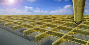 |
| With a special mode of electrohydrodynamic ink-jet printing scientists can create a grid of ultra fine gold walls. Visualisations: Ben Newton / Digit Works |
Abstract:
From smartphones to the operating interfaces of ticket machines and cash dispensers, every touchscreen we use requires transparent electrodes: The devices' glass surface is coated with a barely visible pattern made of conductive material. It is because of this that the devices recognise whether and where exactly a finger is touching the surface.
Nanowalls for smartphones
Zurich, Switzerland | Posted on January 6th, 2016Researchers under the direction of Dimos Poulikakos, Professor of Thermodynamics, have now used 3D print technology to create a new type of transparent electrode, which takes the form of a grid made of gold or silver "nanowalls" on a glass surface. The walls are so thin that they can hardly be seen with the naked eye. It is the first time that scientists have created nanowalls like these using 3D printing. The new electrodes have a higher conductivity and are more transparent than those made of indium tin oxide, the standard material used in smartphones and tablets today. This is a clear advantage: The more transparent the electrodes, the better the screen quality. And the more conductive they are, the more quickly and precisely the touchscreen will work.
Third dimension
"Indium tin oxide is used because the material has a relatively high degree of transparency and the production of thin layers has been well researched, but it is only moderately conductive," says Patrik Rohner, a PhD student in Poulikakos' team. In order to produce more conductive electrodes, the ETH researchers opted for gold and silver, which conduct electricity much better. But because these metals are not transparent, the scientists had to make use of the third dimension. ETH professor Poulikakos explains: "If you want to achieve both high conductivity and transparency in wires made from these metals, you have a conflict of objectives. As the cross-sectional area of gold and silver wires grows, the conductivity increases, but the grid's transparency decreases."
The solution was to use metal walls only 80 to 500 nanometres thick, which are almost invisible when viewed from above. Because they are two to four times taller than they are wide, the cross-sectional area, and thus the conductivity, is sufficiently high.
Ink-jet printer with tiny print head
The researchers produced these tiny metal walls using a printing process known as Nanodrip, which Poulikakos and his colleagues developed three years ago. Its basic principle is a process called electrohydrodynamic ink-jet printing. In this process scientists use inks made from metal nanoparticles in a solvent; an electrical field draws ultra-small droplets of the metallic ink out of a glass capillary. The solvent evaporates quickly, allowing a three-dimensional structure to be built up drop by drop.
What is special about the Nanodrip process is that the droplets that come out of the glass capillary are about ten times smaller than the aperture itself. This allows for much smaller structures to be printed. "Imagine a water drop hanging from a tap that is turned off. And now imagine that another tiny droplet is hanging from this drop - we are only printing the tiny droplet," Poulikakos explains. The researchers managed to create this special form of droplet by perfectly balancing the composition of metallic ink and the electromagnetic field used.
Cost-efficient production
The next big challenge will now be to upscale the method and develop the print process further so that it can be implemented on an industrial scale. To achieve this, the scientists are working with colleagues from ETH spin-off company Scrona.
They have no doubt that once it is upscaled, the technology will bring a host of advantages compared with existing methods. In particular, it will likely be more cost-efficient, as Nanodrip printing, unlike the production of indium tin oxide electrodes, does not require a cleanroom environment. The new electrodes should also be more suitable for large touchscreens due to their higher conductivity. And finally the process is also the first to allow you to vary the height of the nanowalls directly while printing, says ETH PhD student Rohner.
Another possible future application could be in solar cells, where transparent electrodes are also required. The more transparent and conductive they are, the more electricity that can be harnessed. And lastly, the electrodes could also play a role in the further development of curved display using OLED technology.
####
For more information, please click here
Contacts:
Dimos Poulikakos
41-446-322-738
Copyright © ETH Zurich
If you have a comment, please Contact us.Issuers of news releases, not 7th Wave, Inc. or Nanotechnology Now, are solely responsible for the accuracy of the content.
Bookmark:


| Related Links |
| Related News Press |
News and information
![]() Simulating magnetization in a Heisenberg quantum spin chain April 5th, 2024
Simulating magnetization in a Heisenberg quantum spin chain April 5th, 2024
![]() NRL charters Navy�s quantum inertial navigation path to reduce drift April 5th, 2024
NRL charters Navy�s quantum inertial navigation path to reduce drift April 5th, 2024
![]() Discovery points path to flash-like memory for storing qubits: Rice find could hasten development of nonvolatile quantum memory April 5th, 2024
Discovery points path to flash-like memory for storing qubits: Rice find could hasten development of nonvolatile quantum memory April 5th, 2024
![]() Good as gold - improving infectious disease testing with gold nanoparticles April 5th, 2024
Good as gold - improving infectious disease testing with gold nanoparticles April 5th, 2024
Display technology/LEDs/SS Lighting/OLEDs
![]() Utilizing palladium for addressing contact issues of buried oxide thin film transistors April 5th, 2024
Utilizing palladium for addressing contact issues of buried oxide thin film transistors April 5th, 2024
![]() Light guide plate based on perovskite nanocomposites November 3rd, 2023
Light guide plate based on perovskite nanocomposites November 3rd, 2023
![]() Simple ballpoint pen can write custom LEDs August 11th, 2023
Simple ballpoint pen can write custom LEDs August 11th, 2023
Discoveries
![]() Chemical reactions can scramble quantum information as well as black holes April 5th, 2024
Chemical reactions can scramble quantum information as well as black holes April 5th, 2024
![]() New micromaterial releases nanoparticles that selectively destroy cancer cells April 5th, 2024
New micromaterial releases nanoparticles that selectively destroy cancer cells April 5th, 2024
![]() Utilizing palladium for addressing contact issues of buried oxide thin film transistors April 5th, 2024
Utilizing palladium for addressing contact issues of buried oxide thin film transistors April 5th, 2024
Materials/Metamaterials/Magnetoresistance
![]() Nanoscale CL thermometry with lanthanide-doped heavy-metal oxide in TEM March 8th, 2024
Nanoscale CL thermometry with lanthanide-doped heavy-metal oxide in TEM March 8th, 2024
![]() Focused ion beam technology: A single tool for a wide range of applications January 12th, 2024
Focused ion beam technology: A single tool for a wide range of applications January 12th, 2024
Announcements
![]() NRL charters Navy�s quantum inertial navigation path to reduce drift April 5th, 2024
NRL charters Navy�s quantum inertial navigation path to reduce drift April 5th, 2024
![]() Discovery points path to flash-like memory for storing qubits: Rice find could hasten development of nonvolatile quantum memory April 5th, 2024
Discovery points path to flash-like memory for storing qubits: Rice find could hasten development of nonvolatile quantum memory April 5th, 2024
Interviews/Book Reviews/Essays/Reports/Podcasts/Journals/White papers/Posters
![]() Simulating magnetization in a Heisenberg quantum spin chain April 5th, 2024
Simulating magnetization in a Heisenberg quantum spin chain April 5th, 2024
![]() Discovery points path to flash-like memory for storing qubits: Rice find could hasten development of nonvolatile quantum memory April 5th, 2024
Discovery points path to flash-like memory for storing qubits: Rice find could hasten development of nonvolatile quantum memory April 5th, 2024
Energy
![]() Development of zinc oxide nanopagoda array photoelectrode: photoelectrochemical water-splitting hydrogen production January 12th, 2024
Development of zinc oxide nanopagoda array photoelectrode: photoelectrochemical water-splitting hydrogen production January 12th, 2024
![]() Shedding light on unique conduction mechanisms in a new type of perovskite oxide November 17th, 2023
Shedding light on unique conduction mechanisms in a new type of perovskite oxide November 17th, 2023
![]() Inverted perovskite solar cell breaks 25% efficiency record: Researchers improve cell efficiency using a combination of molecules to address different November 17th, 2023
Inverted perovskite solar cell breaks 25% efficiency record: Researchers improve cell efficiency using a combination of molecules to address different November 17th, 2023
![]() The efficient perovskite cells with a structured anti-reflective layer � another step towards commercialization on a wider scale October 6th, 2023
The efficient perovskite cells with a structured anti-reflective layer � another step towards commercialization on a wider scale October 6th, 2023
Solar/Photovoltaic
![]() Development of zinc oxide nanopagoda array photoelectrode: photoelectrochemical water-splitting hydrogen production January 12th, 2024
Development of zinc oxide nanopagoda array photoelectrode: photoelectrochemical water-splitting hydrogen production January 12th, 2024
![]() Shedding light on unique conduction mechanisms in a new type of perovskite oxide November 17th, 2023
Shedding light on unique conduction mechanisms in a new type of perovskite oxide November 17th, 2023
![]() Inverted perovskite solar cell breaks 25% efficiency record: Researchers improve cell efficiency using a combination of molecules to address different November 17th, 2023
Inverted perovskite solar cell breaks 25% efficiency record: Researchers improve cell efficiency using a combination of molecules to address different November 17th, 2023
![]() Charged �molecular beasts� the basis for new compounds: Researchers at Leipzig University use �aggressive� fragments of molecular ions for chemical synthesis November 3rd, 2023
Charged �molecular beasts� the basis for new compounds: Researchers at Leipzig University use �aggressive� fragments of molecular ions for chemical synthesis November 3rd, 2023
|
|
||
|
|
||
| The latest news from around the world, FREE | ||
|
|
||
|
|
||
| Premium Products | ||
|
|
||
|
Only the news you want to read!
Learn More |
||
|
|
||
|
Full-service, expert consulting
Learn More |
||
|
|
||