Home > Press > Leti Develops Local-strain Techniques in FD-SOI Fabrication To Improve Next-Generation Performance, Energy Use
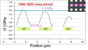 |
| SSDM 2015: Stress profile from 2D Raman extractions for Si MESAs after BOX creep process with 50 nm thick SiN |
Abstract:
CEA-Leti today announced it has developed two techniques to induce local strain in FD-SOI processes for next-generation FD-SOI circuits that will produce more speed at the same, or lower, power consumption, and improve performance.
Leti Develops Local-strain Techniques in FD-SOI Fabrication To Improve Next-Generation Performance, Energy Use
Grenoble, France | Posted on December 8th, 2015The local-strain solutions are dual-strained technologies: compressive SiGe for PFETs and tensile Si for NFETs. In addition to clearing the path to improved performance in FD-SOI technology, they preserve its excellent electrostatic integrity and its in situ performance tunability, due to back biasing.
The two techniques Leti developed can induce local stress as high as 1.6 GPa in the MOSFETs channel.
The first relies on strain transfer from a relaxed SiGe layer on top of SOI film. In a recent paper in the ECS Journal of Solid State Science and Technology, Leti researcher Sylvain Maitrejean described how with this technique he was able to boost the short-channel electron mobility by more than 20 percent compared to unstrained reference. This shows significant promise for enhancing the on-state currents of CMOS transistors and thus for improving the circuit�s speed.
The second technique is closer to strain memorization methods and relies on the ability of the BOX to creep under high-temperature annealing. At SSDM 2015 in Japan, Leti researchers showed that with this local-stress technique they can turn regular unstrained SOI structures into tensile strained Si (sSOI), for NFET areas. Moreover, this �BOX-creep� process also can also be applied to compressive strain creation, as presented at the 2015 Silicon Nanoelectronics Workshop (SNW) conference.
Strained channels enable an increase in the on-state current of CMOS transistors. As a result, the corresponding IC circuits can deliver more speed at the same power, or reduced consumed power and longer battery life at the same performance.
They also have been proven to be an effective way to increase performance of n and p MOSFET transistors via mobility enhancement of electrons and holes. These kinds of techniques enable boosting of the carrier transport in the CMOS channels, and thus increasing the on-state currents. Beginning with the 90nm node, this strain option has been one of the main approaches of the microelectronics industry for improving the IC speed in bulk transistors. While it was not necessary at the 28nm node for FD-SOI, it becomes mandatory beyond the 22/20nm node.
�Leti has continuously focused on improving and fine-tuning FD-SOI technology�s inherent advantages, since pioneering the technology 20 years ago,� said Maud Vinet, head of Leti�s Advanced CMOS Laboratory. �These two new techniques broaden the capabilities of Leti�s FD-SOI platform for next-generation devices, and further position the technology to be a vital part of the Internet of Things and electronics products of the future.�
####
About CEA Leti
As one of three advanced-research institutes within the CEA Technological Research Division, CEA Tech-Leti serves as a bridge between basic research and production of micro- and nanotechnologies that improve the lives of people around the world. It is committed to creating innovation and transferring it to industry. Backed by its portfolio of 2,800 patents, Leti partners with large industrials, SMEs and startups to tailor advanced solutions that strengthen their competitive positions. It has launched 54 startups. Its 8,500m� of new-generation cleanroom space feature 200mm and 300mm wafer processing of micro and nano solutions for applications ranging from space to smart devices. With a staff of more than 1,800, Leti is based in Grenoble, France, and has offices in Silicon Valley, Calif., and Tokyo. Follow us at www.leti.fr and @CEA_Leti.
For more information, please click here
Contacts:
Agency
+33 6 74 93 23 47
Copyright © CEA Leti
If you have a comment, please Contact us.Issuers of news releases, not 7th Wave, Inc. or Nanotechnology Now, are solely responsible for the accuracy of the content.
Bookmark:


| Related News Press |
News and information
![]() Simulating magnetization in a Heisenberg quantum spin chain April 5th, 2024
Simulating magnetization in a Heisenberg quantum spin chain April 5th, 2024
![]() NRL charters Navy�s quantum inertial navigation path to reduce drift April 5th, 2024
NRL charters Navy�s quantum inertial navigation path to reduce drift April 5th, 2024
![]() Discovery points path to flash-like memory for storing qubits: Rice find could hasten development of nonvolatile quantum memory April 5th, 2024
Discovery points path to flash-like memory for storing qubits: Rice find could hasten development of nonvolatile quantum memory April 5th, 2024
Chip Technology
![]() Discovery points path to flash-like memory for storing qubits: Rice find could hasten development of nonvolatile quantum memory April 5th, 2024
Discovery points path to flash-like memory for storing qubits: Rice find could hasten development of nonvolatile quantum memory April 5th, 2024
![]() Utilizing palladium for addressing contact issues of buried oxide thin film transistors April 5th, 2024
Utilizing palladium for addressing contact issues of buried oxide thin film transistors April 5th, 2024
![]() HKUST researchers develop new integration technique for efficient coupling of III-V and silicon February 16th, 2024
HKUST researchers develop new integration technique for efficient coupling of III-V and silicon February 16th, 2024
Nanoelectronics
![]() Interdisciplinary: Rice team tackles the future of semiconductors Multiferroics could be the key to ultralow-energy computing October 6th, 2023
Interdisciplinary: Rice team tackles the future of semiconductors Multiferroics could be the key to ultralow-energy computing October 6th, 2023
![]() Key element for a scalable quantum computer: Physicists from Forschungszentrum J�lich and RWTH Aachen University demonstrate electron transport on a quantum chip September 23rd, 2022
Key element for a scalable quantum computer: Physicists from Forschungszentrum J�lich and RWTH Aachen University demonstrate electron transport on a quantum chip September 23rd, 2022
![]() Reduced power consumption in semiconductor devices September 23rd, 2022
Reduced power consumption in semiconductor devices September 23rd, 2022
![]() Atomic level deposition to extend Moore�s law and beyond July 15th, 2022
Atomic level deposition to extend Moore�s law and beyond July 15th, 2022
Discoveries
![]() Chemical reactions can scramble quantum information as well as black holes April 5th, 2024
Chemical reactions can scramble quantum information as well as black holes April 5th, 2024
![]() New micromaterial releases nanoparticles that selectively destroy cancer cells April 5th, 2024
New micromaterial releases nanoparticles that selectively destroy cancer cells April 5th, 2024
![]() Utilizing palladium for addressing contact issues of buried oxide thin film transistors April 5th, 2024
Utilizing palladium for addressing contact issues of buried oxide thin film transistors April 5th, 2024
Announcements
![]() NRL charters Navy�s quantum inertial navigation path to reduce drift April 5th, 2024
NRL charters Navy�s quantum inertial navigation path to reduce drift April 5th, 2024
![]() Discovery points path to flash-like memory for storing qubits: Rice find could hasten development of nonvolatile quantum memory April 5th, 2024
Discovery points path to flash-like memory for storing qubits: Rice find could hasten development of nonvolatile quantum memory April 5th, 2024
|
|
||
|
|
||
| The latest news from around the world, FREE | ||
|
|
||
|
|
||
| Premium Products | ||
|
|
||
|
Only the news you want to read!
Learn More |
||
|
|
||
|
Full-service, expert consulting
Learn More |
||
|
|
||