Home > Press > IRT Nanoelec Partners Achieve 3D Chip-stacking Technology & 3D Network-on-chip Framework for Digital Processing
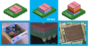 |
| Top: Stacking of 1 die, or 2 or 4 dice in a package Bottom: 3DNoC chip: demonstration platform, package cross section, package on board |
Abstract:
IRT Nanoelec, an R&D consortium focused on Information and Communication Technologies (ICT) using micro- and nanoelectronics, and its partners CEA-Leti, STMicroelectronics and Mentor Graphics have realized an innovative 3D chip called “3DNoC” to demonstrate the use of 3D stacking technology in scalable, complex digital systems-on-chip (SoCs).
IRT Nanoelec Partners Achieve 3D Chip-stacking Technology & 3D Network-on-chip Framework for Digital Processing
Grenoble, France | Posted on July 9th, 2015The 3DNoC chip is based on a 2D die that can be used in a stand-alone applicative mode, and also in a 3D stack with several dice, to multiply the processing performance of the system. The project’s complete demonstration platform shows both the simulated and measured thermal effects in the 3D chip using a new Mentor Graphics® Calibre® thermal-analysis prototype.
“The technology developed for this realization can be easily used and transferred to address mixed-technology applications, such as imagers and RF transceivers, or complex digital processing, such as high-performance computing and programmable devices,” said Severine Cheramy, IRT 3D program director. “In parallel with these results, we are working on developments that address more fine-pitch 3D technology than those used in the 3DNoC demonstrator and solutions for thermal dissipation, temporary bonding and stress issues.”
3D-stacking technology is a promising solution to improve both performance and density integration without requiring transition to the next technology node. It allows the integration of different technologies and simplifies the use of small-sized dice to improve modularity and increase yield. In a complex and traditional 2D SoC, the technology node is defined by the most complex function, and reuse methodology is done at the IP level. A 3D system blends several technologies and reuse methodology can be performed at the elementary die, the “chiplet.”
The 3DNoC chip was defined and designed by Leti, with the direct support of STMicroelectronics, using a specific add-on 3D design kit and a set of 3D sign-off verification tools provided by Mentor Graphics. CMOS technology, 3D technology and packaging were realized by ST and Leti, with a “via-middle option” in 65nm CMOS technology. The test and demonstration platform is a joint development among the three partners.
Proving the viability of 3D stacking
IRT Nanoelec provides a multi-skill environment – including technology development, innovative processing architecture, and specific design tools in a global system- methodology approach – for the development of pioneer 3D demonstrators to prove the viability of 3D stacking in a wide range of applications. Although the 3DNoC chip addresses baseband processing, all technology and design bricks are reusable across a range of other applications.
3DNoC is the first worldwide realization of a 3D-scalable processor chip. It goes beyond prior state-of-the-art as a 3D asynchronous communication network that can exploit the maximum performance of vertical links and offer an aggregate 3D network link bandwidth of 450 MByte/s. The strategy, which is based on increasing the performance of a system by stacking several identical dice in the same footprint, is very similar to HMC or HBM memories. In the case of DRAM, byte capacity is multiplied by the number of elementary dice stacked; the 3DNoC circuit multiplies processing performance.
The Technology
Several identical 65nm CMOS digital dice can be bonded using a face-to-back technology to build a stack of processing elements, using 10µm-diameter through-silicon via (TSV) and 20µm-diameter µpillars and µbumps. In the IRT Nanoelec demonstration, two dice are stacked.
At the elementary die level, provisions were made to allow the stacking of up to four dice: the number of power connections is dimensioned in this way, while the number of signals is constant regardless of the number of stacked dice. Area occupied by the 2,000 TSVs represents about 1 percent of the whole die area (72 mm2) and wafers are thinned to 80µm for TSV revelation at the backside.
3DNoC is mounted in a 581-ball, 0.3mm-pitch BGA package using a stacking-last approach, i.e. the bottom die is bonded on the substrate and after the top one on the bottom.
Targeting digital baseband processing
The digital modules embedded in 3DNoC are computing-intensive IPs, processor cores and programmable DMA engines connected to the NoC routers using a dedicated interface compatible with a packet-switching mechanism.
The global architecture was partitioned in a scalable way to address several modes, depending on the number of antennae used for transmitting-and-receiving levels. The modular elementary die was sized to fit the processing performance required to support the single antenna mode and, by stacking two or four dice, more complex multiple antenna modes are supported. As an example, the 3DNoC chip developed in this project can support up to two antennae for both TX and RX.
Network on Chip (NoC)
For many years, network-on-chip (NoC) has played a key role in 2D complex SoCs, thanks to its ability to efficiently manage data exchanges between many IPs. The fact that packet switching communication is well decoupled to computing IPs makes the extension of the interconnection capabilities to the third dimension easy and natural. The elementary die of the 3DNoC integrates four 3D routers to ensure vertical communication.
Redundancy and fault-tolerance are used in the 3DNoC circuit at both communication and processing levels. Using asynchronous logic for router implementation allows implementing robust 3D communication interfaces without any delay assumption, and makes dynamic voltage and frequency scaling (DVFS) for power optimization easier, relative to processing requirements and thermal constraints. Specific analysis and sizing tools developed by Mentor Graphics for power and thermal aspects were very helpful to architects in the 3D floor plan of the 3DNoC chip. More specifically, the Calibre® 3DSTACK tool has been used for final sign-off verification of the 3D assembly of the two dice.
Several modules have been designed to ensure 3D signal integrity between the different tiers: micro-buffers, ESD protection, 3D link redundancy and data coding. A complete design-for-test methodology has been set up to perform a hierarchical test of each module, tier and stack before and after stacking based on the Mentor Graphics Tessent® test tool suite including test pattern generation.
Mentor Graphics, Calibre, and Tessent are registered trademarks of Mentor Graphics Corporation. All other company or product names are the registered trademarks or trademarks of their respective owners.
####
About IRT Nanoelec
Nanoelec Research Technological Institute (IRT), headed by CEA-Leti, conducts research and development in the field of information and communication technologies (ICT) and, specifically, micro- and nanoelectronics. Working within the framework of programs with investments on future technologies, it leverages Grenoble’s proven innovation ecosystem to create the technologies that will power the nanoelectronics of tomorrow, drive new product development and inspire new applications – like the Internet of Things – for existing technologies. The R&D conducted at IRT Nanoelec provides early insight into how emerging technologies such as 3D integration and silicon photonics will affect integrated circuits.
In addition to its R&D activities, IRT Nanoelec runs a technology-transfer program set up to ensure that the innovations developed directly benefit businesses — especially small and mid-sized businesses — in all industries. IRT Nanoelec also offers educational and training programs to develop the micro- and nanoelectronics competencies businesses will need to remain competitive in tomorrow’s global markets.
For more information, please click here
Contacts:
Didier Louis
+33 6 32 44 64 31
Copyright © IRT Nanoelec
If you have a comment, please Contact us.Issuers of news releases, not 7th Wave, Inc. or Nanotechnology Now, are solely responsible for the accuracy of the content.
Bookmark:


| Related News Press |
News and information
![]() Simulating magnetization in a Heisenberg quantum spin chain April 5th, 2024
Simulating magnetization in a Heisenberg quantum spin chain April 5th, 2024
![]() NRL charters Navy’s quantum inertial navigation path to reduce drift April 5th, 2024
NRL charters Navy’s quantum inertial navigation path to reduce drift April 5th, 2024
![]() Discovery points path to flash-like memory for storing qubits: Rice find could hasten development of nonvolatile quantum memory April 5th, 2024
Discovery points path to flash-like memory for storing qubits: Rice find could hasten development of nonvolatile quantum memory April 5th, 2024
Hardware
![]() The present and future of computing get a boost from new research July 21st, 2023
The present and future of computing get a boost from new research July 21st, 2023
![]() A Carbon Nanotube Microprocessor Mature Enough to Say Hello: Three new breakthroughs make commercial nanotube processors possible March 2nd, 2020
A Carbon Nanotube Microprocessor Mature Enough to Say Hello: Three new breakthroughs make commercial nanotube processors possible March 2nd, 2020
![]() Powering the future: Smallest all-digital circuit opens doors to 5 nm next-gen semiconductor February 11th, 2020
Powering the future: Smallest all-digital circuit opens doors to 5 nm next-gen semiconductor February 11th, 2020
Chip Technology
![]() Discovery points path to flash-like memory for storing qubits: Rice find could hasten development of nonvolatile quantum memory April 5th, 2024
Discovery points path to flash-like memory for storing qubits: Rice find could hasten development of nonvolatile quantum memory April 5th, 2024
![]() Utilizing palladium for addressing contact issues of buried oxide thin film transistors April 5th, 2024
Utilizing palladium for addressing contact issues of buried oxide thin film transistors April 5th, 2024
![]() HKUST researchers develop new integration technique for efficient coupling of III-V and silicon February 16th, 2024
HKUST researchers develop new integration technique for efficient coupling of III-V and silicon February 16th, 2024
Announcements
![]() NRL charters Navy’s quantum inertial navigation path to reduce drift April 5th, 2024
NRL charters Navy’s quantum inertial navigation path to reduce drift April 5th, 2024
![]() Discovery points path to flash-like memory for storing qubits: Rice find could hasten development of nonvolatile quantum memory April 5th, 2024
Discovery points path to flash-like memory for storing qubits: Rice find could hasten development of nonvolatile quantum memory April 5th, 2024
Alliances/Trade associations/Partnerships/Distributorships
![]() Chicago Quantum Exchange welcomes six new partners highlighting quantum technology solutions, from Chicago and beyond September 23rd, 2022
Chicago Quantum Exchange welcomes six new partners highlighting quantum technology solutions, from Chicago and beyond September 23rd, 2022
![]() University of Illinois Chicago joins Brookhaven Lab's Quantum Center June 10th, 2022
University of Illinois Chicago joins Brookhaven Lab's Quantum Center June 10th, 2022
|
|
||
|
|
||
| The latest news from around the world, FREE | ||
|
|
||
|
|
||
| Premium Products | ||
|
|
||
|
Only the news you want to read!
Learn More |
||
|
|
||
|
Full-service, expert consulting
Learn More |
||
|
|
||