Home > Press > EEJA and Tokyo U Achieve Simultaneous Formation of Contact Electrodes for p-Type and n-Type Organic Semiconductor Crystals Using the Plating Method
 |
Abstract:
Enabling the atmospheric formation of low-contact resistance electrodes and high-mobility high-performance organic transistors that are among the best in the world.
EEJA and Tokyo U Achieve Simultaneous Formation of Contact Electrodes for p-Type and n-Type Organic Semiconductor Crystals Using the Plating Method
Tokyo, Japan | Posted on March 15th, 2015Tanaka Holdings, Co., Ltd. (Head office: Chiyoda-ku, Tokyo; President & CEO: Akira Tanae) announced today that Electroplating Engineers of Japan, Ltd. (Plant and Office: Hiratsuka-shi, Kanagawa; President and CEO: Koichiro Tanaka; EEJA), which operates the Tanaka Precious Metals Group's plating business, together with Professor Junichi Takeya of the University of Tokyo's Graduate School of Frontier Sciences, has achieved the world's first success in the development of technology for the simultaneous formation of contact electrodes for p-type and n-type*1 Organic-semiconductor Field Effect Transistors ("OFET," hereafter) using an electroless plating process.
By using an electroless gold plating process with silver nanoparticles as a catalyst for an organic semiconductor, this technology enables the formation in the atmosphere of top contact-type OFET (figure 1)*2 contact electrodes without the use of a vacuum environment, which requires large-scale equipment. As opposed to metallic ink, which has the same atmospheric contact formation, this technology realizes the formation of a high-performance OFET as there is little damage to the organic semiconductor, and the performance of the high-mobility*3 organic semiconductor is not affected. Also, due to the emergence of high-performance n-type semiconductor materials in recent years, more advanced organic electronic devices can now be formed at a low-cost thanks to the simultaneous formation of contact electrodes for p-type and n-type OFET mixed circuits, for which development is speeding up.
For p-type organic semiconductors, the contact resistance of the contact electrodes using this technology is 0.1Kiloohm-cm or less, which is the lowest value currently on record in terms of the contact resistance of organic semiconductor contact electrodes formed in the atmosphere. The atmospheric formation of a high-performance OFET (Figure 2) with low-contact resistance electrodes and high-mobility that are among the top levels in the world is achieved by combining the merits of this technology with those of high-performance coating-type organic semiconductors developed by Professor Takeya which can be formed atmospherically. This result enables the atmospheric formation of organic electronic devices with high-speed drives, and it enables the production of high functionality electronic devices using printed electronics*4.
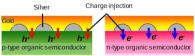
This technology is a process for the formation of contact electrodes with a gold-silver hybrid structure, which is achieved by applying a silver catalyst solution for plating that includes silver nanoparticles to an organic semiconductor crystal, after which a gold coating is applied to the substrate by immersing it in an electroless gold plating solution so that the gaps between the silver grains are filled with gold. This enables the single-process formation of low-contact resistance contact electrodes for p-type organic semiconductors, which facilitate a charge injection from gold, and n-type organic semiconductors, which facilitate a charge injection from silver (Figure 3).
EEJA will announce the research findings relating to this technology at the 62nd Jpan Society of Applied Physics Spring Meeting, to be held between March 11 and March 14 at Tokai University, Shonan Campus (Hiratsuka-shi, Kanagawa).
Background to this technology
OFET is a transistor that uses an organic semiconductor, which means that - among other characteristics unique to organic materials - it can be formed at low-temperatures, is lightweight and is flexible. The high-performance of organic semiconductor materials has progressed rapidly in recent years, and materials are being developed with double-digit increases over the figure that was thought to be the limit for the mobility of organic semiconductors. The pioneering findings of Professor Takeya's research group make possible the atmospheric formation of high-mobility organic semiconductors, which is expected to increase the fields of use for organic semiconductors.
While there are several methods for the formation of OFET contact electrodes, they all suffer from such issues as requiring a vacuum environment and causing damage to organic semiconductors. For example, thin film electrodes can be formed uniformly using the vacuum deposition method, but the equipment used to create a vacuum environment is incredibly expensive, and the loss of materials is huge. Also, while electrode formation in the atmosphere is possible using metallic ink and metallic paste, it also requires the inclusion of organic solvents, high-temperature sintering, and hardening by means of ultra-violet rays, which damages the organic semiconductor, and does not achieve sufficient results as a transistor.
This is why, in September 2014, EEJA together with Professor Takeya's research group jointly developed plating-process contact electrode formation technology for p-type organic semiconductors. In order to stably form electrodes for organic semiconductor crystals, EEJA developed new gold nanoparticles as an electroless plating catalyst. The contact resistance of the contact electrodes formed using this technology is 0.7Kiloohm-cm, which is a remarkably low contact resistance for atmospheric formation contact electrodes. Also, Professor Takeya's research group developed a coating-type organic semiconductor that could be formed in a short time in the atmosphere with a large-surface thin film with uniform crystal orientation, and a mobility (which is the deciding factor in the performance of semiconductors) that greatly surpasses that of conventional organic semiconductors at 10cm2/Vs or more.
Contributing to the development of new devices with OFET application - the development for the future
Because OFET has the characteristics of being printable, lightweight and flexible, we anticipate such device developments as flexible displays and disposable RFID (automatic wireless identification) tags. Currently, development is mainly progressing for devices that use p-type organic semiconductors, but the development of all-flexible displays and wearable computers, which require advanced circuitry and bendable driver ICs, also requires p-type and n-type OFET mixed circuitry and both OFETs must operate at high speeds. This jointly developed technology contributes to technical innovation in connection to organic electronic devices. EEJA will continue to find further solutions for utilization in organic electronic devices.
*1 p-type organic semiconductors and n-type organic semiconductors
Organic compounds crystalized with uniform crystal orientation acquire the characteristics of a semiconductor. By injecting a positive charge, the electrified object is referred to as a p- (positive) type organic semiconductor. By injecting a negative charge, the electrified object is referred to as an n- (negative) type organic semiconductor. The metal that is easier to be injected with a charge varies depending on whether it is a p-type or n-type.
*2 Top contact-type OFET
This is an organic transistor where the contact electrodes are located on the semiconductor crystal. This structure enables a drive with a higher speed than that of OFETs with other structures. However, because the electrodes are formed after forming the organic semiconductor crystal, the organic semiconductor is easily damaged, and contact electrodes are difficult to form.
*3 Mobility
This signifies the ease of movement for the charge within the semiconductor. Electronic devices that carry out complex processes require a higher mobility. Until a few years ago, the mobility of organic semiconductors was generally about 0.1cm2/Vs, but materials have been developed in recent years with a mobility of 10cm2/Vs or more.
*4 Printed electronics
This is a technology for the atmospheric formation of electronic circuits and devices on substrates using printing technology and so on.
####
About Tanaka Holdings, Co., Ltd.
Tanaka Holdings Co., Ltd. (Holding company of Tanaka Precious Metals)
Headquarters: 22F, Tokyo Building, 2-7-3 Marunouchi, Chiyoda-ku, Tokyo
Representative: Akira Tanae, President & CEO
Founded: 1885
Incorporated: 1918
Capital: 500 million yen
Employees in consolidated group: 3,562 (FY2013)
Net sales of consolidated group: 967.6 billion yen (FY2013)
Main businesses of the group: Manufacture, sales, import and export of precious metals (platinum, gold, silver, and others) and various types of industrial precious metals products. Recycling and refining of precious metals.
Website: http://www.tanaka.co.jp/english (Tanaka Precious Metals), http://pro.tanaka.co.jp/en (Industrial products)
Electroplating Engineers of Japan Ltd. (EEJA)
Head office: 5-50 Shinmachi, Hiratsuka-shi, Kanagawa
Representative: Koichiro Tanaka, President & CEO
Established: 1965
Capital: 100 million yen
Employees: 94 (FY2013)
Sales: 23,360 million yen (FY2013)
Areas of Business:
1. Development, production, sales and export of Sel-Rex precious metal and base metal plating
solutions, additives, and surface processing-related chemicals through a technical
partnership with the Enthone Group
2. Development, production, sales, and export of plating equipment
3. Import and sales of plating-related products
Website: www.eeja.com/
About the Tanaka Precious Metals
Established in 1885, the Tanaka Precious Metals has built a diversified range of business activities focused on the use of precious metals. On April 1, 2010, the group was reorganized with Tanaka Holdings Co., Ltd. as the holding company (parent company) of the Tanaka Precious Metals. In addition to strengthening corporate governance, the company aims to improve overall service to customers by ensuring efficient management and dynamic execution of operations. Tanaka Precious Metals is committed, as a specialist corporate entity, to providing a diverse range of products through cooperation among group companies.
Tanaka Precious Metals is in the top class in Japan in terms of the volume of precious metal handled, and for many years the group has developed and stably supplied industrial precious metals, in addition to providing accessories and savings commodities utilizing precious metals. As precious metal professionals, the Group will continue to contribute to enriching people's lives in the future.
The eight core companies in the Tanaka Precious Metals are as follows.
- Tanaka Holdings Co., Ltd. (pure holding company)
- Tanaka Kikinzoku Kogyo K.K.
- Tanaka Kikinzoku Hanbai K.K.
- Tanaka Kikinzoku International K.K.
- Tanaka Denshi Kogyo K.K.
- Electroplating Engineers of Japan, Limited
- Tanaka Kikinzoku Jewelry K.K.
- Tanaka Kikinzoku Business Service K.K.
For more information, please click here
Contacts:
Global Sales Dept.
Tanaka Kikinzoku International K.K. (TKI)
https://www.tanaka.co.jp/support/req/ks_contact_e/index.html
Copyright © Tanaka Holdings, Co., Ltd.
If you have a comment, please Contact us.Issuers of news releases, not 7th Wave, Inc. or Nanotechnology Now, are solely responsible for the accuracy of the content.
Bookmark:


| Related News Press |
News and information
![]() Simulating magnetization in a Heisenberg quantum spin chain April 5th, 2024
Simulating magnetization in a Heisenberg quantum spin chain April 5th, 2024
![]() NRL charters Navy�s quantum inertial navigation path to reduce drift April 5th, 2024
NRL charters Navy�s quantum inertial navigation path to reduce drift April 5th, 2024
![]() Discovery points path to flash-like memory for storing qubits: Rice find could hasten development of nonvolatile quantum memory April 5th, 2024
Discovery points path to flash-like memory for storing qubits: Rice find could hasten development of nonvolatile quantum memory April 5th, 2024
Chip Technology
![]() Discovery points path to flash-like memory for storing qubits: Rice find could hasten development of nonvolatile quantum memory April 5th, 2024
Discovery points path to flash-like memory for storing qubits: Rice find could hasten development of nonvolatile quantum memory April 5th, 2024
![]() Utilizing palladium for addressing contact issues of buried oxide thin film transistors April 5th, 2024
Utilizing palladium for addressing contact issues of buried oxide thin film transistors April 5th, 2024
![]() HKUST researchers develop new integration technique for efficient coupling of III-V and silicon February 16th, 2024
HKUST researchers develop new integration technique for efficient coupling of III-V and silicon February 16th, 2024
Discoveries
![]() Chemical reactions can scramble quantum information as well as black holes April 5th, 2024
Chemical reactions can scramble quantum information as well as black holes April 5th, 2024
![]() New micromaterial releases nanoparticles that selectively destroy cancer cells April 5th, 2024
New micromaterial releases nanoparticles that selectively destroy cancer cells April 5th, 2024
![]() Utilizing palladium for addressing contact issues of buried oxide thin film transistors April 5th, 2024
Utilizing palladium for addressing contact issues of buried oxide thin film transistors April 5th, 2024
Announcements
![]() NRL charters Navy�s quantum inertial navigation path to reduce drift April 5th, 2024
NRL charters Navy�s quantum inertial navigation path to reduce drift April 5th, 2024
![]() Discovery points path to flash-like memory for storing qubits: Rice find could hasten development of nonvolatile quantum memory April 5th, 2024
Discovery points path to flash-like memory for storing qubits: Rice find could hasten development of nonvolatile quantum memory April 5th, 2024
Research partnerships
![]() Discovery points path to flash-like memory for storing qubits: Rice find could hasten development of nonvolatile quantum memory April 5th, 2024
Discovery points path to flash-like memory for storing qubits: Rice find could hasten development of nonvolatile quantum memory April 5th, 2024
![]() Researchers� approach may protect quantum computers from attacks March 8th, 2024
Researchers� approach may protect quantum computers from attacks March 8th, 2024
![]() 'Sudden death' of quantum fluctuations defies current theories of superconductivity: Study challenges the conventional wisdom of superconducting quantum transitions January 12th, 2024
'Sudden death' of quantum fluctuations defies current theories of superconductivity: Study challenges the conventional wisdom of superconducting quantum transitions January 12th, 2024
|
|
||
|
|
||
| The latest news from around the world, FREE | ||
|
|
||
|
|
||
| Premium Products | ||
|
|
||
|
Only the news you want to read!
Learn More |
||
|
|
||
|
Full-service, expert consulting
Learn More |
||
|
|
||