Home > Press > Graphenea granted patent on graphene transfer
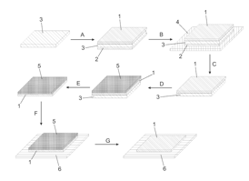 |
| Figure: A sketch of the steps in the transfer process. The method starts from two sheets of graphene grown on both sides of a metal (typically copper) foil (step A in the figure). The CVD process necessarily yields graphene on both layers of the copper, and the first step in the transfer process is to remove one of the layers. In Graphenea�s patent, this step is performed with a thermal release tape. Using pneumatic cylinders and accuracy valves, thermal release adhesive tape is rolled onto the graphene surface, smoothly following the topology of the underlying copper, without any air bubbles (step B). Next, the stack is heated to release the tape, which pulls along the graphene layer. Left behind is a clean film of copper with a layer of graphene on top (C). The subsequent steps involve depositing a sacrificial protective layer (commonly a polymer such as PMMA) on top of the graphene (D), etching away the copper with a solution of iron chloride (E), mechanically transferring the graphene onto the desired substrate (F), and disso lving the protective layer (G). This method results in graphene films of excellent quality, generally surpassing that of films obtained by other transfer and etching methods. With this patent Graphenea hopes to further strengthen its position as a leader of the graphene industry. |
Abstract:
Graphenea was granted a patent for a method of transfer of large-area graphene. In particular, the patent refers to transferring graphene grown by chemical vapor deposition (CVD) from a metal foil to an insulating substrate. As CVD is the most promising way of growing large, high quality graphene sheets, which are most often useful only on insulating substrates, this could be a key patent in the graphene industry. The granted patent is the first for Graphenea.
Graphenea granted patent on graphene transfer
San Sebastian, Spain | Posted on February 9th, 2015Graphene, possessing a vast array of exotic properties such as high electronic mobility, extraordinary thermal conductivity, great strength, flexibility, and transparency, is an ideal candidate for a wide variety of novel applications. If all the unusually excellent properties of graphene are industrially exploited, the material could have applications in electronics (high frequency devices, transistors, etc.), energy (solar cells, batteries, supercapacitors, etc.), touch screen and display technology (TV screens, mobile phones, etc.), sensors, and other technologies. To access graphene's superior properties, however, one needs to obtain large high-quality sheets of it.
The most appropriate known method of obtaining such large sheets is CVD. In CVD a source of carbon is introduced into a chamber holding a metal catalyst substrate. Under specific controlled conditions (pressure, temperature), the carbon forms smooth single atomic layers on all sides of the metal foil. CVD growth of graphene has, since its introduction in 2009, been optimized and perfected, already in 2010 featuring 30-inch graphene layers. More than 95% coverage of the substrate can be obtained on copper.
After growth on a metal, the graphene in most cases needs to be transferred to a useful substrate, such as an insulator (SOI). Transfer of such a large yet thin film is obviously a challenge which often results in an imperfect final product. Thus, to fully unlock the potential of CVD growth, the transfer method needed to be optimized.
US patent number 20140001152, entitled "Method of manufacturing a graphene monolayer on insulating substrates", describes the procedure by which Graphenea makes some of the world's highest quality large-area graphene on arbitrary substrates.
####
About Graphenea Inc.
Graphenea, headquartered at the nanotechnology cluster CIC nanoGune in San Sebastian, Spain, was established in 2010, and has since grown to be one of the world's largest providers of graphene. Graphenea employs 12 people and exports graphene materials tomore than 370 customers in 53 countries. The company has focused on developing the CVD growth and transfer method, reaching a consistently high quality of its graphene films that researchers can rely on. Graphenea employs a team of skilled laboratory staff who have brought graphene transfer techniques to a new level, offering the same high quality films on any substrate. Following the trends in cutting-edge research, Graphenea also produces chemically exfoliated graphene, in volumes up to 2,5 litres per package. Graphenea partners with large multinationals to develop custom graphene materials for their applications.
Its research agility and ability to keep pace with the progress of graphene science and technology has allowed Graphenea to become the largest graphene supplier in the Graphene Flagship, a ten year project of the European Commission worth a billion euros. The company keeps a close relation with the world's leading scientists, regularly publishing scientific articles of the highest level.
For more information, please click here
Contacts:
Graphenea
Avenida de Tolosa, 76
20018 - Donostia/San Sebasti�n
Spain
Contact:
Webpage: www.graphenea.com
Media contact:
Marko Spasenovic
Copyright © Graphenea
If you have a comment, please Contact us.Issuers of news releases, not 7th Wave, Inc. or Nanotechnology Now, are solely responsible for the accuracy of the content.
Bookmark:


| Related News Press |
News and information
![]() Simulating magnetization in a Heisenberg quantum spin chain April 5th, 2024
Simulating magnetization in a Heisenberg quantum spin chain April 5th, 2024
![]() NRL charters Navy�s quantum inertial navigation path to reduce drift April 5th, 2024
NRL charters Navy�s quantum inertial navigation path to reduce drift April 5th, 2024
![]() Discovery points path to flash-like memory for storing qubits: Rice find could hasten development of nonvolatile quantum memory April 5th, 2024
Discovery points path to flash-like memory for storing qubits: Rice find could hasten development of nonvolatile quantum memory April 5th, 2024
Graphene/ Graphite
![]() NRL discovers two-dimensional waveguides February 16th, 2024
NRL discovers two-dimensional waveguides February 16th, 2024
Announcements
![]() NRL charters Navy�s quantum inertial navigation path to reduce drift April 5th, 2024
NRL charters Navy�s quantum inertial navigation path to reduce drift April 5th, 2024
![]() Discovery points path to flash-like memory for storing qubits: Rice find could hasten development of nonvolatile quantum memory April 5th, 2024
Discovery points path to flash-like memory for storing qubits: Rice find could hasten development of nonvolatile quantum memory April 5th, 2024
Patents/IP/Tech Transfer/Licensing
![]() Getting drugs across the blood-brain barrier using nanoparticles March 3rd, 2023
Getting drugs across the blood-brain barrier using nanoparticles March 3rd, 2023
![]() Metasurfaces control polarized light at will: New research unlocks the hidden potential of metasurfaces August 13th, 2021
Metasurfaces control polarized light at will: New research unlocks the hidden potential of metasurfaces August 13th, 2021
![]() Arrowhead Pharmaceuticals Announces Closing of Agreement with Takeda November 27th, 2020
Arrowhead Pharmaceuticals Announces Closing of Agreement with Takeda November 27th, 2020
|
|
||
|
|
||
| The latest news from around the world, FREE | ||
|
|
||
|
|
||
| Premium Products | ||
|
|
||
|
Only the news you want to read!
Learn More |
||
|
|
||
|
Full-service, expert consulting
Learn More |
||
|
|
||