Home > Press > Advance brings 'hyperbolic metamaterials' closer to reality
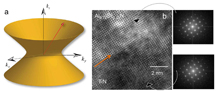 |
| "Hyperbolic metamaterials" could bring optical advances including powerful microscopes, quantum computers and high-performance solar cells. The graphic at left depicts a metamaterial's "hyperbolic dispersion" of light. At center is a high-resolution transmission electron microscope image showing the interface of titanium nitride and aluminum scandium nitride in a "superlattice" that is promising for potential applications. At right are two images created using a method called fast Fourier transform to see individual layers in the material. Purdue University image |
Abstract:
Epitaxial superlattices with titanium nitride as a plasmonic component for optical hyperbolic metamaterials
Gururaj V. Naik,1 Bivas Saha,2 Jing Liu,3 Sammy M. Saber,2 Eric Stach,2 Joseph MK Irudayaraj,3 Timothy D. Sands,1,2 Vladimir M. Shalaev1 and Alexandra Boltasseva*,1,4
1 School of Electrical and Computer Engineering, and Birck Nanotechnology Center, Purdue
University
2 School of Materials Engineering, and Birck Nanotechnology Center, Purdue University
3 Department of Agricultural and Biological Engineering, and Bindley Bioscience Center,
Purdue University
4 DTU Fotonik, Department of Photonics Engineering, Technical University of Denmark CORRESPONDING AUTHOR: *Alexandra Boltasseva
Titanium nitride (TiN) is a plasmonic material having optical properties resembling gold. Unlike gold however, TiN is CMOS-compatible, mechanically strong, and thermally stable at higher temperatures. Additionally, TiN can be grown in smooth, ultra-thin crystalline films, which are useful in constructing many plasmonic and metamaterial devices including hyperbolic metamaterials (HMMs). Hyperbolic metamaterials have been shown to exhibit exotic optical properties, including extremely high broadband photonic densities of states (PDOS), which are useful in quantum plasmonics applications. However, the extent to which the exotic properties of HMMs can be realized has been seriously limited by fabrication constraints and material properties. Here, we address these issues by realizing an epitaxial superlattice as an HMM. The superlattice consists of ultra-smooth layers as thin as 5 nm and exhibits sharp interfaces, which are essential for high-quality HMM devices. Our study reveals that such a TiN-based superlattice HMM provides a higher PDOS enhancement than gold- or silver-based HMMs. Given the advantages of TiN as a CMOS compatible plasmonic material, this demonstration brings a paradigm shift to the field of metamaterials similar to the way heterostructures did to the field of solid-state light sources.
Advance brings 'hyperbolic metamaterials' closer to reality
West Lafayette, IN | Posted on May 15th, 2014Researchers have taken a step toward practical applications for "hyperbolic metamaterials," ultra-thin crystalline films that could bring optical advances including powerful microscopes, quantum computers and high-performance solar cells.
New developments are reminiscent of advances that ushered in silicon chip technology, said Alexandra Boltasseva, a Purdue University associate professor of electrical and computer engineering.
Optical metamaterials harness clouds of electrons called surface plasmons to manipulate and control light. However, some of the plasmonic components under development rely on the use of metals such as gold and silver, which are incompatible with the complementary metal-oxide-semiconductor (CMOS) manufacturing process used to construct integrated circuits and do not transmit light efficiently.
Now researchers have shown how to create "superlattice" crystals from layers of the metal titanium nitride and aluminum scandium nitride, a dielectric, or insulator. Superlattices are crystals that can be grown continuously by adding new layers, a requirement for practical application.
"This work is a very important step in terms of fundamental contributions in materials science and optics as well as paving the way to some interesting applications," Boltasseva said. "We believe this demonstration brings a paradigm shift to the field of metamaterials similar to developments that led to dramatic advances in silicon technology."
Research findings are detailed in a paper appearing this week in the online Early Edition of Proceedings of the National Academy of Sciences.
Researchers created the superlattices using a method called epitaxy, "growing" the layers inside a vacuum chamber with a technique known as magnetron sputtering. It is difficult to use the technique to create structures that have sharply defined, ultra-thin and ultra-smooth layers of two different materials.
"This is one of the first reports of a metal-dielectric epitaxial superlattice," said Purdue doctoral student Bivas Saha, co-lead author of the PNAS paper with Gururaj V. Naik, a former Purdue doctoral student and now a postdoctoral scholar at Stanford University.
The list of possible applications for metamaterials includes a "planar hyperlens" that could make optical microscopes 10 times more powerful and able to see objects as small as DNA, advanced sensors, more efficient solar collectors, and quantum computing.
"Plasmonic and metamaterial devices require good material building blocks, both plasmonic and dielectric, in order to be useful in any real-world application," Boltasseva said. "Here, we develop both plasmonic and dielectric materials that can be grown epitaxially into ultra-thin and ultra-smooth layers with sharp interfaces."
Metamaterials have engineered surfaces that contain features, patterns or elements, such as tiny antennas or alternating layers of nitrides that enable unprecedented control of light. Under development for about 15 years, the metamaterials owe their unusual potential to precision design on the scale of nanometers.
The PNAS paper was authored by Naik; Saha; doctoral students Jing Liu and Sammy M. Saber; Eric Stach, a researcher at Brookhaven National Laboratory; Joseph Irudayaraj, a professor in Purdue's Department of Agricultural and Biological Engineering; Timothy D. Sands, executive vice president for academic affairs and provost and Basil S. Turner Professor of Engineering in the Schools of Materials Engineering and Electrical and Computer Engineering; Vladimir M. Shalaev, scientific director of nanophotonics at Purdue's Birck Nanotechnology Center and a distinguished professor of electrical and computer engineering; and Boltasseva.
"This work results from a unique collaboration between nanophotonics and materials science," Boltasseva said.
The hyperbolic metamaterial behaves as a metal when light is passing through it in one direction and like a dielectric in the perpendicular direction. This "extreme anisotropy" leads to "hyperbolic dispersion" of light and the ability to extract many more photons from devices than otherwise possible, resulting in high performance.
The layers of titanium nitride and aluminum scandium nitride used in this study are each about 5 to 20 nanometers thick. However, researchers have demonstrated that such superlattices can also be developed where the layers could be as thin as 2 nanometers, a tiny dimension only about eight atoms thick.
"People have tried for more than 50 years to combine metals and semiconductors with atomic-scale precision to build superlattices," Saha said. "However, this is one of the first demonstrations of achieving that step. The fascinating optical properties we see here are a manifestation of extraordinary structural control that we have achieved."
The feat is possible by choosing a metal and dielectric with compatible crystal structures, enabling the layers to grow together as a superlattice. The researchers alloyed aluminum nitride with scandium nitride, meaning the aluminum nitride is impregnated with scandium atoms to alter the material's crystal lattice to match titanium nitride's.
"The possibility of growing both metal and dielectric material components as a whole epitaxial system is indispensable for realizing high-performance metamaterials," Saha said. "One of the stumbling blocks is the fact that common dielectrics such as silica, alumina and other oxides cannot be used in combination with metallic components such as metal nitrides because the deposition processes are not compatible with each other."
Both of the materials should possess the same or compatible crystal structures.
"In general, a lattice mismatch of less than 5 percent is necessary for growing epitaxial quality films," he said.
A U.S. patent application has been filed through the Purdue Office of Technology Commercialization.
The material has been shown to work in a broad spectrum from near-infrared to visible light, potentially promising a wide array of applications.
"That's a novel part of this work - that we can create a superlattice metamaterial showing hyperbolic dispersion in the visible spectrum range," Boltasseva said.
The near-infrared is essential for telecommunications and optical communications, and visible light is important for sensors, microscopes and efficient solid-state light sources.
"Most interesting is the realm of quantum information technology," she said.
Computers based on quantum physics would have quantum bits, or "qubits," that exist in both the on and off states simultaneously, dramatically increasing the computer's power and memory. Quantum computers would take advantage of a phenomenon described by quantum theory called "entanglement." Instead of only the states of one and zero used in conventional computer processing, there are many possible "entangled quantum states" in between one and zero, increasing the capacity to process information.
The research has been funded in part by the U.S. Army Research Office and the National Science Foundation.
####
For more information, please click here
Contacts:
Writer:
Emil Venere
765-494-4709
Sources:
Alexandra Boltasseva
765-494-0301
Bivas Saha
Copyright © Purdue University
If you have a comment, please Contact us.Issuers of news releases, not 7th Wave, Inc. or Nanotechnology Now, are solely responsible for the accuracy of the content.
Bookmark:


| Related News Press |
News and information
![]() Simulating magnetization in a Heisenberg quantum spin chain April 5th, 2024
Simulating magnetization in a Heisenberg quantum spin chain April 5th, 2024
![]() NRL charters Navy�s quantum inertial navigation path to reduce drift April 5th, 2024
NRL charters Navy�s quantum inertial navigation path to reduce drift April 5th, 2024
![]() Discovery points path to flash-like memory for storing qubits: Rice find could hasten development of nonvolatile quantum memory April 5th, 2024
Discovery points path to flash-like memory for storing qubits: Rice find could hasten development of nonvolatile quantum memory April 5th, 2024
![]() Good as gold - improving infectious disease testing with gold nanoparticles April 5th, 2024
Good as gold - improving infectious disease testing with gold nanoparticles April 5th, 2024
Thin films
![]() Utilizing palladium for addressing contact issues of buried oxide thin film transistors April 5th, 2024
Utilizing palladium for addressing contact issues of buried oxide thin film transistors April 5th, 2024
Imaging
![]() Nanoscale CL thermometry with lanthanide-doped heavy-metal oxide in TEM March 8th, 2024
Nanoscale CL thermometry with lanthanide-doped heavy-metal oxide in TEM March 8th, 2024
![]() The USTC realizes In situ electron paramagnetic resonance spectroscopy using single nanodiamond sensors November 3rd, 2023
The USTC realizes In situ electron paramagnetic resonance spectroscopy using single nanodiamond sensors November 3rd, 2023
![]() Observation of left and right at nanoscale with optical force October 6th, 2023
Observation of left and right at nanoscale with optical force October 6th, 2023
Govt.-Legislation/Regulation/Funding/Policy
![]() NRL charters Navy�s quantum inertial navigation path to reduce drift April 5th, 2024
NRL charters Navy�s quantum inertial navigation path to reduce drift April 5th, 2024
![]() Discovery points path to flash-like memory for storing qubits: Rice find could hasten development of nonvolatile quantum memory April 5th, 2024
Discovery points path to flash-like memory for storing qubits: Rice find could hasten development of nonvolatile quantum memory April 5th, 2024
![]() Chemical reactions can scramble quantum information as well as black holes April 5th, 2024
Chemical reactions can scramble quantum information as well as black holes April 5th, 2024
Quantum Computing
![]() Simulating magnetization in a Heisenberg quantum spin chain April 5th, 2024
Simulating magnetization in a Heisenberg quantum spin chain April 5th, 2024
![]() Discovery points path to flash-like memory for storing qubits: Rice find could hasten development of nonvolatile quantum memory April 5th, 2024
Discovery points path to flash-like memory for storing qubits: Rice find could hasten development of nonvolatile quantum memory April 5th, 2024
![]() With VECSELs towards the quantum internet Fraunhofer: IAF achieves record output power with VECSEL for quantum frequency converters April 5th, 2024
With VECSELs towards the quantum internet Fraunhofer: IAF achieves record output power with VECSEL for quantum frequency converters April 5th, 2024
![]() Chemical reactions can scramble quantum information as well as black holes April 5th, 2024
Chemical reactions can scramble quantum information as well as black holes April 5th, 2024
Discoveries
![]() Chemical reactions can scramble quantum information as well as black holes April 5th, 2024
Chemical reactions can scramble quantum information as well as black holes April 5th, 2024
![]() New micromaterial releases nanoparticles that selectively destroy cancer cells April 5th, 2024
New micromaterial releases nanoparticles that selectively destroy cancer cells April 5th, 2024
![]() Utilizing palladium for addressing contact issues of buried oxide thin film transistors April 5th, 2024
Utilizing palladium for addressing contact issues of buried oxide thin film transistors April 5th, 2024
Materials/Metamaterials/Magnetoresistance
![]() Nanoscale CL thermometry with lanthanide-doped heavy-metal oxide in TEM March 8th, 2024
Nanoscale CL thermometry with lanthanide-doped heavy-metal oxide in TEM March 8th, 2024
![]() Focused ion beam technology: A single tool for a wide range of applications January 12th, 2024
Focused ion beam technology: A single tool for a wide range of applications January 12th, 2024
Announcements
![]() NRL charters Navy�s quantum inertial navigation path to reduce drift April 5th, 2024
NRL charters Navy�s quantum inertial navigation path to reduce drift April 5th, 2024
![]() Discovery points path to flash-like memory for storing qubits: Rice find could hasten development of nonvolatile quantum memory April 5th, 2024
Discovery points path to flash-like memory for storing qubits: Rice find could hasten development of nonvolatile quantum memory April 5th, 2024
Interviews/Book Reviews/Essays/Reports/Podcasts/Journals/White papers/Posters
![]() Simulating magnetization in a Heisenberg quantum spin chain April 5th, 2024
Simulating magnetization in a Heisenberg quantum spin chain April 5th, 2024
![]() Discovery points path to flash-like memory for storing qubits: Rice find could hasten development of nonvolatile quantum memory April 5th, 2024
Discovery points path to flash-like memory for storing qubits: Rice find could hasten development of nonvolatile quantum memory April 5th, 2024
Tools
![]() Ferroelectrically modulate the Fermi level of graphene oxide to enhance SERS response November 3rd, 2023
Ferroelectrically modulate the Fermi level of graphene oxide to enhance SERS response November 3rd, 2023
![]() The USTC realizes In situ electron paramagnetic resonance spectroscopy using single nanodiamond sensors November 3rd, 2023
The USTC realizes In situ electron paramagnetic resonance spectroscopy using single nanodiamond sensors November 3rd, 2023
Patents/IP/Tech Transfer/Licensing
![]() Getting drugs across the blood-brain barrier using nanoparticles March 3rd, 2023
Getting drugs across the blood-brain barrier using nanoparticles March 3rd, 2023
![]() Metasurfaces control polarized light at will: New research unlocks the hidden potential of metasurfaces August 13th, 2021
Metasurfaces control polarized light at will: New research unlocks the hidden potential of metasurfaces August 13th, 2021
![]() Arrowhead Pharmaceuticals Announces Closing of Agreement with Takeda November 27th, 2020
Arrowhead Pharmaceuticals Announces Closing of Agreement with Takeda November 27th, 2020
Military
![]() NRL charters Navy�s quantum inertial navigation path to reduce drift April 5th, 2024
NRL charters Navy�s quantum inertial navigation path to reduce drift April 5th, 2024
![]() What heat can tell us about battery chemistry: using the Peltier effect to study lithium-ion cells March 8th, 2024
What heat can tell us about battery chemistry: using the Peltier effect to study lithium-ion cells March 8th, 2024
![]() New chip opens door to AI computing at light speed February 16th, 2024
New chip opens door to AI computing at light speed February 16th, 2024
Energy
![]() Development of zinc oxide nanopagoda array photoelectrode: photoelectrochemical water-splitting hydrogen production January 12th, 2024
Development of zinc oxide nanopagoda array photoelectrode: photoelectrochemical water-splitting hydrogen production January 12th, 2024
![]() Shedding light on unique conduction mechanisms in a new type of perovskite oxide November 17th, 2023
Shedding light on unique conduction mechanisms in a new type of perovskite oxide November 17th, 2023
![]() Inverted perovskite solar cell breaks 25% efficiency record: Researchers improve cell efficiency using a combination of molecules to address different November 17th, 2023
Inverted perovskite solar cell breaks 25% efficiency record: Researchers improve cell efficiency using a combination of molecules to address different November 17th, 2023
![]() The efficient perovskite cells with a structured anti-reflective layer � another step towards commercialization on a wider scale October 6th, 2023
The efficient perovskite cells with a structured anti-reflective layer � another step towards commercialization on a wider scale October 6th, 2023
Photonics/Optics/Lasers
![]() With VECSELs towards the quantum internet Fraunhofer: IAF achieves record output power with VECSEL for quantum frequency converters April 5th, 2024
With VECSELs towards the quantum internet Fraunhofer: IAF achieves record output power with VECSEL for quantum frequency converters April 5th, 2024
![]() Nanoscale CL thermometry with lanthanide-doped heavy-metal oxide in TEM March 8th, 2024
Nanoscale CL thermometry with lanthanide-doped heavy-metal oxide in TEM March 8th, 2024
![]() Optically trapped quantum droplets of light can bind together to form macroscopic complexes March 8th, 2024
Optically trapped quantum droplets of light can bind together to form macroscopic complexes March 8th, 2024
![]() HKUST researchers develop new integration technique for efficient coupling of III-V and silicon February 16th, 2024
HKUST researchers develop new integration technique for efficient coupling of III-V and silicon February 16th, 2024
Solar/Photovoltaic
![]() Development of zinc oxide nanopagoda array photoelectrode: photoelectrochemical water-splitting hydrogen production January 12th, 2024
Development of zinc oxide nanopagoda array photoelectrode: photoelectrochemical water-splitting hydrogen production January 12th, 2024
![]() Shedding light on unique conduction mechanisms in a new type of perovskite oxide November 17th, 2023
Shedding light on unique conduction mechanisms in a new type of perovskite oxide November 17th, 2023
![]() Inverted perovskite solar cell breaks 25% efficiency record: Researchers improve cell efficiency using a combination of molecules to address different November 17th, 2023
Inverted perovskite solar cell breaks 25% efficiency record: Researchers improve cell efficiency using a combination of molecules to address different November 17th, 2023
![]() Charged �molecular beasts� the basis for new compounds: Researchers at Leipzig University use �aggressive� fragments of molecular ions for chemical synthesis November 3rd, 2023
Charged �molecular beasts� the basis for new compounds: Researchers at Leipzig University use �aggressive� fragments of molecular ions for chemical synthesis November 3rd, 2023
Quantum nanoscience
![]() Simulating magnetization in a Heisenberg quantum spin chain April 5th, 2024
Simulating magnetization in a Heisenberg quantum spin chain April 5th, 2024
![]() Optically trapped quantum droplets of light can bind together to form macroscopic complexes March 8th, 2024
Optically trapped quantum droplets of light can bind together to form macroscopic complexes March 8th, 2024
![]() Bridging light and electrons January 12th, 2024
Bridging light and electrons January 12th, 2024
![]() 'Sudden death' of quantum fluctuations defies current theories of superconductivity: Study challenges the conventional wisdom of superconducting quantum transitions January 12th, 2024
'Sudden death' of quantum fluctuations defies current theories of superconductivity: Study challenges the conventional wisdom of superconducting quantum transitions January 12th, 2024
|
|
||
|
|
||
| The latest news from around the world, FREE | ||
|
|
||
|
|
||
| Premium Products | ||
|
|
||
|
Only the news you want to read!
Learn More |
||
|
|
||
|
Full-service, expert consulting
Learn More |
||
|
|
||