Home > Press > Playing pool with carbon atoms: UA physicists discover how to change the crystal structure of graphene
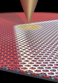 |
| Using a sharp metal scanning tunneling microscopy tip, LeRoy and his collaborators were able to move the domain border between the two graphene configurations around.
Credit: Pablo San-Jose ICMM-CSI |
Abstract:
A University of Arizona-led team of physicists has discovered how to change the crystal structure of graphene, more commonly known as pencil lead, with an electric field, an important step toward the possible use of graphene in microprocessors that would be smaller and faster than current, silicon-based technology.
Playing pool with carbon atoms: UA physicists discover how to change the crystal structure of graphene
Tucson, AZ | Posted on April 30th, 2014Graphene consists of extremely thin sheets of graphite: when writing with a pencil, graphene sheets slough off the pencil's graphite core and stick to the page. If placed under a high-powered electron microscope, graphene reveals its sheet-like structure of cross-linked carbon atoms, resembling chicken wire.
When manipulated by an electric field, parts of the material are transformed from behaving as a metal to behaving as a semiconductor, the UA physicists found.
Graphene is the world's thinnest material, with 300,000 sheets needed to amount to the thickness of a human hair or a sheet of paper. Scientists and engineers are interested in it because of its possible applications in microelectronic devices, in hopes of propelling us from the silicon age to the graphene age. The tricky part is to control the flow of electrons through the material, a necessary prerequisite for putting it to work in any type of electronic circuit.
Brian LeRoy, UA associate professor of physics, and his collaborators have cleared a hurdle toward that goal by showing that an electric field is capable of controlling the crystal structure of trilayer graphene - which is made up of three layers of graphene.
Most materials require high temperatures, pressure or both to change their crystal structure, which is the reason why graphite doesn't spontaneously turn into diamond or vice versa.
"It is extremely rare for a material to change its crystal structure just by applying an electric field," LeRoy said. "Making trilayer graphene is an exceptionally unique system that could be utilized to create novel devices."
Trilayer graphene can be stacked in two unique ways. This is analogous to stacking layers of billiards balls in a triangular lattice, with the balls representing the carbon atoms.
"When you stack two layers of billiards balls, their 'crystal structure' is fixed because the top layer of balls must sit in holes formed by the triangles of the bottom layer," explained Matthew Yankowitz, a third-year doctoral student in LeRoy's lab. He is the first author on the published research, which appears in the journal Nature Materials. "The third layer of balls may be stacked in such a way that its balls are flush above the balls in the bottom layer, or it may be offset slightly so its balls come to lie above the holes formed by triangles in the bottom layer."
These two stacking configurations can naturally exist in the same flake of graphene. The two domains are separated by a sharp boundary where the carbon hexagons are strained to accommodate the transition from one stacking pattern to the other.
"Due to the different stacking configurations on either side of the domain wall, one side of the material behaves as a metal, while the other side behaves as a semiconductor," LeRoy explained.
While probing the domain wall with an electric field, applied by an extremely sharp metal scanning tunneling microscopy tip, the researchers in LeRoy's group discovered that they could move the position of the domain wall within the flake of graphene. And as they moved the domain wall, the crystal structure of the trilayer graphene changed in its wake.
"We had the idea that there would be interesting electronic effects at the boundary, and the boundary kept moving around on us," LeRoy said. "At first it was frustrating, but once we realized what was going on, it turned out to be the most interesting effect."
By applying an electric field to move the boundary, it is now possible for the first time to change the crystal structure of graphene in a controlled fashion.
"Now we have a knob that we can turn to change the material from metallic into semiconducting and vice versa to control the flow of electrons," LeRoy said. "It basically gives us an on-off switch, which had not been realized yet in graphene."
While more research is needed before graphene can be applied in technological applications on an industrial scale, researchers see ways it may be used.
"If you used a wide electrode instead of a pointed tip, you could move the boundary between the two configurations a farther distance, which could make it possible to create transistors from graphene," Yankowitz said.
Transistors are a staple of electronic circuits because they control the flow of electrons.
Unlike silicon transistors used now, graphene-based transistors could be extremely thin, making the device much smaller, and since electrons move through graphene much faster than through silicon, the devices would enable faster computing.
In addition, silicon-based transistors are being manufactured to function as one of two types - p-type or n-type - whereas graphene could operate as both. This would make them cheaper to produce and more versatile in their applications.
###
The other contributors to the research paper, "Electric field control of soliton motion and stacking in trilayer graphene," include Joel I-Jan Wang (Massachusetts Institute of Technology and Harvard University in Cambridge, Massachusetts), A. Glen Birdwell (U.S. Army Research Laboratory, Adelphi, Maryland), Yu-An Chen (MIT), K. Watanabe and T. Taniguchi (National Institute for Materials Science, Tsukuba, Japan), Philippe Jacquod (UA Department of Physics), Pablo San-Jose (Instituto de Ciencia de Materiales de Madrid) and Pablo Jarillo-Herrero (MIT).
####
For more information, please click here
Contacts:
Daniel Stolte
520-626-4402
Copyright © University of Arizona
If you have a comment, please Contact us.Issuers of news releases, not 7th Wave, Inc. or Nanotechnology Now, are solely responsible for the accuracy of the content.
Bookmark:


| Related Links |
![]() The study appears in the advance online publication of Nature Materials at:
The study appears in the advance online publication of Nature Materials at:
| Related News Press |
News and information
![]() Simulating magnetization in a Heisenberg quantum spin chain April 5th, 2024
Simulating magnetization in a Heisenberg quantum spin chain April 5th, 2024
![]() NRL charters Navy�s quantum inertial navigation path to reduce drift April 5th, 2024
NRL charters Navy�s quantum inertial navigation path to reduce drift April 5th, 2024
![]() Discovery points path to flash-like memory for storing qubits: Rice find could hasten development of nonvolatile quantum memory April 5th, 2024
Discovery points path to flash-like memory for storing qubits: Rice find could hasten development of nonvolatile quantum memory April 5th, 2024
Graphene/ Graphite
![]() NRL discovers two-dimensional waveguides February 16th, 2024
NRL discovers two-dimensional waveguides February 16th, 2024
Laboratories
![]() A battery�s hopping ions remember where they�ve been: Seen in atomic detail, the seemingly smooth flow of ions through a battery�s electrolyte is surprisingly complicated February 16th, 2024
A battery�s hopping ions remember where they�ve been: Seen in atomic detail, the seemingly smooth flow of ions through a battery�s electrolyte is surprisingly complicated February 16th, 2024
![]() NRL discovers two-dimensional waveguides February 16th, 2024
NRL discovers two-dimensional waveguides February 16th, 2024
Govt.-Legislation/Regulation/Funding/Policy
![]() NRL charters Navy�s quantum inertial navigation path to reduce drift April 5th, 2024
NRL charters Navy�s quantum inertial navigation path to reduce drift April 5th, 2024
![]() Discovery points path to flash-like memory for storing qubits: Rice find could hasten development of nonvolatile quantum memory April 5th, 2024
Discovery points path to flash-like memory for storing qubits: Rice find could hasten development of nonvolatile quantum memory April 5th, 2024
![]() Chemical reactions can scramble quantum information as well as black holes April 5th, 2024
Chemical reactions can scramble quantum information as well as black holes April 5th, 2024
Chip Technology
![]() Discovery points path to flash-like memory for storing qubits: Rice find could hasten development of nonvolatile quantum memory April 5th, 2024
Discovery points path to flash-like memory for storing qubits: Rice find could hasten development of nonvolatile quantum memory April 5th, 2024
![]() Utilizing palladium for addressing contact issues of buried oxide thin film transistors April 5th, 2024
Utilizing palladium for addressing contact issues of buried oxide thin film transistors April 5th, 2024
![]() HKUST researchers develop new integration technique for efficient coupling of III-V and silicon February 16th, 2024
HKUST researchers develop new integration technique for efficient coupling of III-V and silicon February 16th, 2024
Discoveries
![]() Chemical reactions can scramble quantum information as well as black holes April 5th, 2024
Chemical reactions can scramble quantum information as well as black holes April 5th, 2024
![]() New micromaterial releases nanoparticles that selectively destroy cancer cells April 5th, 2024
New micromaterial releases nanoparticles that selectively destroy cancer cells April 5th, 2024
![]() Utilizing palladium for addressing contact issues of buried oxide thin film transistors April 5th, 2024
Utilizing palladium for addressing contact issues of buried oxide thin film transistors April 5th, 2024
Announcements
![]() NRL charters Navy�s quantum inertial navigation path to reduce drift April 5th, 2024
NRL charters Navy�s quantum inertial navigation path to reduce drift April 5th, 2024
![]() Discovery points path to flash-like memory for storing qubits: Rice find could hasten development of nonvolatile quantum memory April 5th, 2024
Discovery points path to flash-like memory for storing qubits: Rice find could hasten development of nonvolatile quantum memory April 5th, 2024
Interviews/Book Reviews/Essays/Reports/Podcasts/Journals/White papers/Posters
![]() Simulating magnetization in a Heisenberg quantum spin chain April 5th, 2024
Simulating magnetization in a Heisenberg quantum spin chain April 5th, 2024
![]() Discovery points path to flash-like memory for storing qubits: Rice find could hasten development of nonvolatile quantum memory April 5th, 2024
Discovery points path to flash-like memory for storing qubits: Rice find could hasten development of nonvolatile quantum memory April 5th, 2024
Tools
![]() Ferroelectrically modulate the Fermi level of graphene oxide to enhance SERS response November 3rd, 2023
Ferroelectrically modulate the Fermi level of graphene oxide to enhance SERS response November 3rd, 2023
![]() The USTC realizes In situ electron paramagnetic resonance spectroscopy using single nanodiamond sensors November 3rd, 2023
The USTC realizes In situ electron paramagnetic resonance spectroscopy using single nanodiamond sensors November 3rd, 2023
Military
![]() NRL charters Navy�s quantum inertial navigation path to reduce drift April 5th, 2024
NRL charters Navy�s quantum inertial navigation path to reduce drift April 5th, 2024
![]() What heat can tell us about battery chemistry: using the Peltier effect to study lithium-ion cells March 8th, 2024
What heat can tell us about battery chemistry: using the Peltier effect to study lithium-ion cells March 8th, 2024
![]() New chip opens door to AI computing at light speed February 16th, 2024
New chip opens door to AI computing at light speed February 16th, 2024
Research partnerships
![]() Discovery points path to flash-like memory for storing qubits: Rice find could hasten development of nonvolatile quantum memory April 5th, 2024
Discovery points path to flash-like memory for storing qubits: Rice find could hasten development of nonvolatile quantum memory April 5th, 2024
![]() Researchers� approach may protect quantum computers from attacks March 8th, 2024
Researchers� approach may protect quantum computers from attacks March 8th, 2024
![]() 'Sudden death' of quantum fluctuations defies current theories of superconductivity: Study challenges the conventional wisdom of superconducting quantum transitions January 12th, 2024
'Sudden death' of quantum fluctuations defies current theories of superconductivity: Study challenges the conventional wisdom of superconducting quantum transitions January 12th, 2024
|
|
||
|
|
||
| The latest news from around the world, FREE | ||
|
|
||
|
|
||
| Premium Products | ||
|
|
||
|
Only the news you want to read!
Learn More |
||
|
|
||
|
Full-service, expert consulting
Learn More |
||
|
|
||