Home > Press > Chemnitz and Jena (Germany) Fraunhofer ENAS orders a Variable Shaped Beam Lithography System from Vistec Electron Beam for Advanced Research
 |
Abstract:
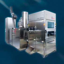
Vistec Electron Beam GmbH, a leading supplier of electron-beam lithography systems, announced that Fraunhofer ENAS in Chemnitz has purchased a Variable Shaped Beam system Vistec SB254. The Fraunhofer Institute for Electronic Nano Systems ENAS, a leading research center within Germany's Fraunhofer-Gesellschaft, will utilize the new electron-beam lithography system for their micro and nano technologies in a wide range of applications.
Chemnitz and Jena (Germany) Fraunhofer ENAS orders a Variable Shaped Beam Lithography System from Vistec Electron Beam for Advanced Research
Jena, Germany | Posted on February 25th, 2014The Fraunhofer ENAS owns an excellent technological know-how in the field of smart systems integration, micro and nano systems and micro and nano electronics. The core competencies comprise design, development, test and evaluation of reliability of components and systems, interconnect technologies as well as system integration. "The new electron-beam lithography system was chosen due to its operational flexibility and capacity to handle a large variety of different materials, high performance accuracy combined with a top level of automation. These features are essential to fulfill the requirements of our customers and partners in research and industry.", states Professor Dr. Thomas Gessner, Director of Fraunhofer ENAS.
The Fraunhofer ENAS purchase decision has been based on the result of an European tendering procedure including an intensive evaluation.
The Vistec SB254 is a high performance, cost-effective and universal electron-beam lithography system, enabling the usage for both direct write and mask making for a large variety of applications in industry and applied research.
The system is capable of handling and exposing transparent and non-transparent materials which are widely used in semiconductor and optical applications. Equipped with 50 kV Variable Shaped Beam electron optics, an address grid of 1 nm and an exposure platform with a stage travel range of 210 mm x 210 mm this system enables lithography below 20nm on various substrates from pieces up to 200 mm wafers and 7 inch masks.
As an optional feature, Cell Projection is also available. A Graphical User Interface (GUI) and fully automated cassette-to-cassette substrate handling, including substrate pre-alignment, allow the effective usage in an environment with consistently changing requirements. Furthermore the system features the data preparation software package ePLACE (provided by EQUIcon Software GmbH).
"We are very pleased, that Fraunhofer ENAS placed the order with Vistec. The installation of the new Vistec SB254 constitutes a new level of collaboration which started more than 20 years ago." comments Wolfgang Dorl, General Manager of Vistec Electron Beam.
####
About Vistec Electron Beam GmbH
Vistec Electron Beam GmbH provides leading technology solutions for advanced electron-beam lithography. Based on the Variable Shaped Beam (VSB) principle, the electron-beam lithography systems are mainly utilized for semiconductor applications and advanced research such as silicon direct write, compound semiconductor, mask making, integrated optics and several new emerging markets.
The company is located in Jena, Germany. In addition to its production facility in Germany, Vistec Electron Beam maintains service and support centers in Europe and Taiwan.
About Fraunhofer ENAS
The product and service portfolio of the Fraunhofer Institute for Electronic Nano Systems ENAS covers high-precision sensors for industrial applications, sensor and actuator systems with control units and evaluation electronics, printed functionalities like antennas and batteries as well as material and reliability research for microelectronics and micro system technology. The development, the design and the test of MEMS/NEMS, methods and technologies for their encapsulation and integration with electronics as well as micro and nano electronics and 3D integration are especially in the focus of the work. Application areas are semiconductor industry, medical engineering, mechanical engineering, automotive industry, logistics as well as aeronautics.
For more information, please click here
Contacts:
Dr. Martina Vogel
Fraunhofer ENAS
Officer of the executive director and manager marketing / PR
Technologie-Campus 3
09126 Chemnitz (Germany)
Phone: +49(0) 371 45001 203
Fax: +49(0) 371 45001 303
http://www.enas.fraunhofer.de/
Ines Stolberg
Vistec Electron Beam GmbH
Manager Strategic Marketing
Ilmstr. 4
D-07743 Jena (Germany)
Tel.: +49(0)3641/7998 155
Fax: +49(0)3641/7998 222
www.vistec-semi.com
PR Agency
Tower PR
Leutragraben 1
D-07743 Jena (Germany)
Tel.: +49(0)3641/8761182
www.tower-pr.com
Copyright © Vistec Electron Beam GmbH
If you have a comment, please Contact us.Issuers of news releases, not 7th Wave, Inc. or Nanotechnology Now, are solely responsible for the accuracy of the content.
Bookmark:


| Related News Press |
News and information
![]() Simulating magnetization in a Heisenberg quantum spin chain April 5th, 2024
Simulating magnetization in a Heisenberg quantum spin chain April 5th, 2024
![]() NRL charters Navy�s quantum inertial navigation path to reduce drift April 5th, 2024
NRL charters Navy�s quantum inertial navigation path to reduce drift April 5th, 2024
![]() Discovery points path to flash-like memory for storing qubits: Rice find could hasten development of nonvolatile quantum memory April 5th, 2024
Discovery points path to flash-like memory for storing qubits: Rice find could hasten development of nonvolatile quantum memory April 5th, 2024
Chip Technology
![]() Discovery points path to flash-like memory for storing qubits: Rice find could hasten development of nonvolatile quantum memory April 5th, 2024
Discovery points path to flash-like memory for storing qubits: Rice find could hasten development of nonvolatile quantum memory April 5th, 2024
![]() Utilizing palladium for addressing contact issues of buried oxide thin film transistors April 5th, 2024
Utilizing palladium for addressing contact issues of buried oxide thin film transistors April 5th, 2024
![]() HKUST researchers develop new integration technique for efficient coupling of III-V and silicon February 16th, 2024
HKUST researchers develop new integration technique for efficient coupling of III-V and silicon February 16th, 2024
Announcements
![]() NRL charters Navy�s quantum inertial navigation path to reduce drift April 5th, 2024
NRL charters Navy�s quantum inertial navigation path to reduce drift April 5th, 2024
![]() Discovery points path to flash-like memory for storing qubits: Rice find could hasten development of nonvolatile quantum memory April 5th, 2024
Discovery points path to flash-like memory for storing qubits: Rice find could hasten development of nonvolatile quantum memory April 5th, 2024
Tools
![]() Ferroelectrically modulate the Fermi level of graphene oxide to enhance SERS response November 3rd, 2023
Ferroelectrically modulate the Fermi level of graphene oxide to enhance SERS response November 3rd, 2023
![]() The USTC realizes In situ electron paramagnetic resonance spectroscopy using single nanodiamond sensors November 3rd, 2023
The USTC realizes In situ electron paramagnetic resonance spectroscopy using single nanodiamond sensors November 3rd, 2023
New-Contracts/Sales/Customers
![]() Bruker Light-Sheet Microscopes at Major Comprehensive Cancer Center: New Advanced Imaging Center Powered by Two MuVi and LCS SPIM Microscopes March 25th, 2021
Bruker Light-Sheet Microscopes at Major Comprehensive Cancer Center: New Advanced Imaging Center Powered by Two MuVi and LCS SPIM Microscopes March 25th, 2021
![]() Arrowhead Pharmaceuticals Announces Closing of Agreement with Takeda November 27th, 2020
Arrowhead Pharmaceuticals Announces Closing of Agreement with Takeda November 27th, 2020
![]() Veeco Announces Aledia Order of 300mm MOCVD Equipment for microLED Displays: Propel� Platform First 300mm System with EFEM Designed for Advanced Display Applications October 20th, 2020
Veeco Announces Aledia Order of 300mm MOCVD Equipment for microLED Displays: Propel� Platform First 300mm System with EFEM Designed for Advanced Display Applications October 20th, 2020
![]() GREENWAVES TECHNOLOGIES Announces Next Generation GAP9 Hearables Platform Using GLOBALFOUNDRIES 22FDX Solution October 16th, 2020
GREENWAVES TECHNOLOGIES Announces Next Generation GAP9 Hearables Platform Using GLOBALFOUNDRIES 22FDX Solution October 16th, 2020
|
|
||
|
|
||
| The latest news from around the world, FREE | ||
|
|
||
|
|
||
| Premium Products | ||
|
|
||
|
Only the news you want to read!
Learn More |
||
|
|
||
|
Full-service, expert consulting
Learn More |
||
|
|
||