Home > Press > Ballistic transport in graphene suggests new type of electronic device
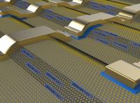 |
| This is a conceptual drawing of an electronic circuit comprised of interconnected graphene nanoribbons (black atoms) that are epitaxially grown on steps etched in silicon carbide (yellow atoms). Electrons (blue) travel ballistically along the ribbon and then from one ribbon to the next via the metal contacts. Electron flow is modulated by electrostatic gates.
Credit: Courtesy of John Hankinson |
Abstract:
Using electrons more like photons could provide the foundation for a new type of electronic device that would capitalize on the ability of graphene to carry electrons with almost no resistance even at room temperature - a property known as ballistic transport.
Ballistic transport in graphene suggests new type of electronic device
Atlanta, GA | Posted on February 5th, 2014Research reported this week shows that electrical resistance in nanoribbons of epitaxial graphene changes in discrete steps following quantum mechanical principles. The research shows that the graphene nanoribbons act more like optical waveguides or quantum dots, allowing electrons to flow smoothly along the edges of the material. In ordinary conductors such as copper, resistance increases in proportion to the length as electrons encounter more and more impurities while moving through the conductor.
The ballistic transport properties, similar to those observed in cylindrical carbon nanotubes, exceed theoretical conductance predictions for graphene by a factor of 10. The properties were measured in graphene nanoribbons approximately 40 nanometers wide that had been grown on the edges of three-dimensional structures etched into silicon carbide wafers.
"This work shows that we can control graphene electrons in very different ways because the properties are really exceptional," said Walt de Heer, a Regent's professor in the School of Physics at the Georgia Institute of Technology. "This could result in a new class of coherent electronic devices based on room temperature ballistic transport in graphene. Such devices would be very different from what we make today in silicon."
The research, which was supported by the National Science Foundation, the Air Force Office of Scientific Research and the W.M. Keck Foundation, was reported February 5 in the journal Nature. The research was done through a collaboration of scientists from Georgia Tech in the United States, Leibniz Universit�t Hannover in Germany, the Centre National de la Recherche Scientifique (CNRS) in France and Oak Ridge National Laboratory in the United States.
For nearly a decade, researchers have been trying to use the unique properties of graphene to create electronic devices that operate much like existing silicon semiconductor chips. But those efforts have met with limited success because graphene - a lattice of carbon atoms that can be made as little as one layer thick - cannot be easily given the electronic bandgap that such devices need to operate.
De Heer argues that researchers should stop trying to use graphene like silicon, and instead use its unique electron transport properties to design new types of electronic devices that could allow ultra-fast computing - based on a new approach to switching. Electrons in the graphene nanoribbons can move tens or hundreds of microns without scattering.
"This constant resistance is related to one of the fundamental constants of physics, the conductance quantum," de Heer said. "The resistance of this channel does not depend on temperature, and it does not depend on the amount of current you are putting through it."
What does disrupt the flow of electrons, however, is measuring the resistance with an electrical probe. The measurements showed that touching the nanoribbons with a single probe doubles the resistance; touching it with two probes triples the resistance.
"The electrons hit the probe and scatter," explained de Heer. "It's a lot like a stream in which water is flowing nicely until you put rocks in the way. We have done systematic studies to show that when you touch the nanoribbons with a probe, you introduce a method for the electrons to scatter, and that changes the resistance."
The nanoribbons are grown epitaxially on silicon carbon wafers into which patterns have been etched using standard microelectronics fabrication techniques. When the wafers are heated to approximately 1,000 degrees Celsius, silicon is preferentially driven off along the edges, forming graphene nanoribbons whose structure is determined by the pattern of the three-dimensional surface. Once grown, the nanoribbons require no further processing.
The advantage of fabricating graphene nanoribbons this way is that it produces edges that are perfectly smooth, annealed by the fabrication process. The smooth edges allow electrons to flow through the nanoribbons without disruption. If traditional etching techniques are used to cut nanoribbons from graphene sheets, the resulting edges are too rough to allow ballistic transport.
"It seems that the current is primarily flowing on the edges," de Heer said. "There are other electrons in the bulk portion of the nanoribbons, but they do not interact with the electrons flowing at the edges."
The electrons on the edge flow more like photons in optical fiber, helping them avoid scattering. "These electrons are really behaving more like light," he said. "It is like light going through an optical fiber. Because of the way the fiber is made, the light transmits without scattering."
Electron mobility measurements surpassing one million correspond to a sheet resistance of one ohm per square that is two orders of magnitude lower than what is observed in two-dimensional graphene - and ten times smaller than the best theoretical predictions for graphene.
"This should enable a new way of doing electronics," de Heer said. "We are already able to steer these electrons and we can switch them using rudimentary means. We can put a roadblock, and then open it up again. New kinds of switches for this material are now on the horizon."
Theoretical explanations for what the researchers have measured are incomplete. De Heer speculates that the graphene nanoribbons may be producing a new type of electronic transport similar to what is observed in superconductors.
"There is a lot of fundamental physics that needs to be done to understand what we are seeing," he added. "We believe this shows that there is a real possibility for a new type of graphene-based electronics."
Georgia Tech researchers have pioneered graphene-based electronics since 2001, for which they hold a patent, filed in 2003. The technique involves etching patterns into electronics-grade silicon carbide wafers, then heating the wafers to drive off silicon, leaving patterns of graphene.
###
In addition to de Heer, the paper's authors included Jens Baringhaus, Frederik Edler and Christoph Tegenkamp from the Institut f�r Festk�rperphysik, Leibniz Universit�t, Hannover in Germany; Edward Conrad, Ming Ruan and Zhigang Jiang from the School of Physics at Georgia Tech; Claire Berger from Georgia Tech and Institut N�el at the Centre National de la Recherche Scientifique (CNRS) in France; Antonio Tejeda and Muriel Sicot from the Institut Jean Lamour, Universite de Nancy, Centre National de la Recherche Scientifique (CNRS) in France; An-Ping Li from the Center for Nanophase Materials Sciences at Oak Ridge National Laboratory, and Amina Taleb-Ibrahimi from the CNRS Synchotron SOLEIL in France.
This research was supported by the National Science Foundation (NSF) Materials Research Science and Engineering Center (MRSEC) at Georgia Tech through award DMR-0820382, the Air Force Office of Scientific Research (AFOSR) and the Partner University Fund from the Embassy of France. Any conclusions or recommendations are those of the authors and do not necessarily represent the official views of the NSF or AFOSR.
####
For more information, please click here
Contacts:
John Toon
404-894-6986
Copyright © Georgia Institute of Technology
If you have a comment, please Contact us.Issuers of news releases, not 7th Wave, Inc. or Nanotechnology Now, are solely responsible for the accuracy of the content.
Bookmark:


| Related Links |
| Related News Press |
Physics
![]() Simulating magnetization in a Heisenberg quantum spin chain April 5th, 2024
Simulating magnetization in a Heisenberg quantum spin chain April 5th, 2024
![]() Nanoscale CL thermometry with lanthanide-doped heavy-metal oxide in TEM March 8th, 2024
Nanoscale CL thermometry with lanthanide-doped heavy-metal oxide in TEM March 8th, 2024
![]() Optically trapped quantum droplets of light can bind together to form macroscopic complexes March 8th, 2024
Optically trapped quantum droplets of light can bind together to form macroscopic complexes March 8th, 2024
News and information
![]() Simulating magnetization in a Heisenberg quantum spin chain April 5th, 2024
Simulating magnetization in a Heisenberg quantum spin chain April 5th, 2024
![]() NRL charters Navy�s quantum inertial navigation path to reduce drift April 5th, 2024
NRL charters Navy�s quantum inertial navigation path to reduce drift April 5th, 2024
![]() Discovery points path to flash-like memory for storing qubits: Rice find could hasten development of nonvolatile quantum memory April 5th, 2024
Discovery points path to flash-like memory for storing qubits: Rice find could hasten development of nonvolatile quantum memory April 5th, 2024
Imaging
![]() Nanoscale CL thermometry with lanthanide-doped heavy-metal oxide in TEM March 8th, 2024
Nanoscale CL thermometry with lanthanide-doped heavy-metal oxide in TEM March 8th, 2024
Graphene/ Graphite
![]() NRL discovers two-dimensional waveguides February 16th, 2024
NRL discovers two-dimensional waveguides February 16th, 2024
Laboratories
![]() A battery�s hopping ions remember where they�ve been: Seen in atomic detail, the seemingly smooth flow of ions through a battery�s electrolyte is surprisingly complicated February 16th, 2024
A battery�s hopping ions remember where they�ve been: Seen in atomic detail, the seemingly smooth flow of ions through a battery�s electrolyte is surprisingly complicated February 16th, 2024
![]() NRL discovers two-dimensional waveguides February 16th, 2024
NRL discovers two-dimensional waveguides February 16th, 2024
Govt.-Legislation/Regulation/Funding/Policy
![]() NRL charters Navy�s quantum inertial navigation path to reduce drift April 5th, 2024
NRL charters Navy�s quantum inertial navigation path to reduce drift April 5th, 2024
![]() Discovery points path to flash-like memory for storing qubits: Rice find could hasten development of nonvolatile quantum memory April 5th, 2024
Discovery points path to flash-like memory for storing qubits: Rice find could hasten development of nonvolatile quantum memory April 5th, 2024
![]() Chemical reactions can scramble quantum information as well as black holes April 5th, 2024
Chemical reactions can scramble quantum information as well as black holes April 5th, 2024
Chip Technology
![]() Discovery points path to flash-like memory for storing qubits: Rice find could hasten development of nonvolatile quantum memory April 5th, 2024
Discovery points path to flash-like memory for storing qubits: Rice find could hasten development of nonvolatile quantum memory April 5th, 2024
![]() Utilizing palladium for addressing contact issues of buried oxide thin film transistors April 5th, 2024
Utilizing palladium for addressing contact issues of buried oxide thin film transistors April 5th, 2024
![]() HKUST researchers develop new integration technique for efficient coupling of III-V and silicon February 16th, 2024
HKUST researchers develop new integration technique for efficient coupling of III-V and silicon February 16th, 2024
Memory Technology
![]() Utilizing palladium for addressing contact issues of buried oxide thin film transistors April 5th, 2024
Utilizing palladium for addressing contact issues of buried oxide thin film transistors April 5th, 2024
![]() Interdisciplinary: Rice team tackles the future of semiconductors Multiferroics could be the key to ultralow-energy computing October 6th, 2023
Interdisciplinary: Rice team tackles the future of semiconductors Multiferroics could be the key to ultralow-energy computing October 6th, 2023
![]() Researchers discover materials exhibiting huge magnetoresistance June 9th, 2023
Researchers discover materials exhibiting huge magnetoresistance June 9th, 2023
Discoveries
![]() Chemical reactions can scramble quantum information as well as black holes April 5th, 2024
Chemical reactions can scramble quantum information as well as black holes April 5th, 2024
![]() New micromaterial releases nanoparticles that selectively destroy cancer cells April 5th, 2024
New micromaterial releases nanoparticles that selectively destroy cancer cells April 5th, 2024
![]() Utilizing palladium for addressing contact issues of buried oxide thin film transistors April 5th, 2024
Utilizing palladium for addressing contact issues of buried oxide thin film transistors April 5th, 2024
Announcements
![]() NRL charters Navy�s quantum inertial navigation path to reduce drift April 5th, 2024
NRL charters Navy�s quantum inertial navigation path to reduce drift April 5th, 2024
![]() Discovery points path to flash-like memory for storing qubits: Rice find could hasten development of nonvolatile quantum memory April 5th, 2024
Discovery points path to flash-like memory for storing qubits: Rice find could hasten development of nonvolatile quantum memory April 5th, 2024
Interviews/Book Reviews/Essays/Reports/Podcasts/Journals/White papers/Posters
![]() Simulating magnetization in a Heisenberg quantum spin chain April 5th, 2024
Simulating magnetization in a Heisenberg quantum spin chain April 5th, 2024
![]() Discovery points path to flash-like memory for storing qubits: Rice find could hasten development of nonvolatile quantum memory April 5th, 2024
Discovery points path to flash-like memory for storing qubits: Rice find could hasten development of nonvolatile quantum memory April 5th, 2024
Tools
![]() Ferroelectrically modulate the Fermi level of graphene oxide to enhance SERS response November 3rd, 2023
Ferroelectrically modulate the Fermi level of graphene oxide to enhance SERS response November 3rd, 2023
![]() The USTC realizes In situ electron paramagnetic resonance spectroscopy using single nanodiamond sensors November 3rd, 2023
The USTC realizes In situ electron paramagnetic resonance spectroscopy using single nanodiamond sensors November 3rd, 2023
Military
![]() NRL charters Navy�s quantum inertial navigation path to reduce drift April 5th, 2024
NRL charters Navy�s quantum inertial navigation path to reduce drift April 5th, 2024
![]() What heat can tell us about battery chemistry: using the Peltier effect to study lithium-ion cells March 8th, 2024
What heat can tell us about battery chemistry: using the Peltier effect to study lithium-ion cells March 8th, 2024
![]() New chip opens door to AI computing at light speed February 16th, 2024
New chip opens door to AI computing at light speed February 16th, 2024
|
|
||
|
|
||
| The latest news from around the world, FREE | ||
|
|
||
|
|
||
| Premium Products | ||
|
|
||
|
Only the news you want to read!
Learn More |
||
|
|
||
|
Full-service, expert consulting
Learn More |
||
|
|
||