Home > Press > ZEISS Crossbeam Sets New Standards in 3D Nanotomography and Nanofabrication: Fast Materials Processing and High Resolution Imaging
 |
Abstract:
ZEISS will be presenting the first system of the new Crossbeam series at the MC 2013 in Regensburg, Germany. Its outstanding features include high speed in materials analysis and processing and its wide diversity of applications. Time intensive 3D experiments that used to run for several days can now be completed overnight.
ZEISS Crossbeam Sets New Standards in 3D Nanotomography and Nanofabrication: Fast Materials Processing and High Resolution Imaging
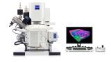
Jena and Regensburg, Germany | Posted on January 22nd, 2014The newly developed focused ion beam (FIB) column enables fast and precise materials processing that can be observed with the field emission scanning electron microscope in real-time. High resolution over the entire voltage and current range allows users to work quickly and precisely. Designed for stability, the system ensures reproducible results even in long-term experiments. The field of application is expanded by the optionally available Massive Ablation Laser that rapidly prepares samples to access deeply buried regions of interest. Crossbeam is suitable for use in both materials and life sciences. Materials scientists benefit from the excellent 3D analytics, the ability to image magnetic and non-conductive specimens with maximum resolution, and from the unique materials contrasts.
Bioscientists can use Crossbeam, above all, for fast tomography series with high Z resolution in cell and tissue biology. The STEM detection module delivers additional structural information. The system offers automated workflows, e.g. for TEM lamella preparation. At the same time, the open software offers users the possibility of integrating and automating their own applications. The modular design of Crossbeam makes it an open 3D nano workstation that can be configured and field-upgraded for a broad spectrum of today's and future applications, therefore offering the user maximum flexibility.
The microscope system is available in two versions. The GEMINI I VP (variable pressure) column of Crossbeam 340 offers optimal analysis conditions for in situ experiments with outgassing and charging specimens. Thanks to the GEMINI II column with double condenser system, Crossbeam 540 users benefit from more information in a shorter time. The system delivers high resolution, even with low voltage and high beam current, enabling fast analytics and ease of use.
In combination with a ZEISS Xradia X-ray microscope (XRM), Crossbeam offers the possibility of complete specimen analysis across several orders of magnitude. The X-ray microscope first provides a 3D image of the specimen without destroying it before the identified areas of interest are processed with the focused ion beam and analyzed with the electron beam.
####
About ZEISS
The Carl Zeiss Group is an international leader in the fields of optics and optoelectronics. In fiscal year 2011/12 the company�s approximately 24,000 employees generated revenue of nearly 4.2 billion euros. In the markets for Industrial Solutions, Research Solutions, Medical Technology and Consumer Optics, ZEISS has contributed to technological progress for more than 160 years and enhances the quality of life of many people around the globe. The Carl Zeiss Group develops and produces planetariums, eyeglass lenses, camera and cine lenses and binoculars as well as solutions for biomedical research, medical technology and the semiconductor, automotive and mechanical engineering industries. ZEISS is present in over 40 countries around the globe with about 40 production facilities, over 50 sales and services locations and approximately 20 research and development sites. Carl Zeiss AG is fully owned by the Carl Zeiss Stiftung (Carl Zeiss Foundation). Founded in 1846 in Jena, the company is headquartered in Oberkochen, Germany.
Microscopy
The Microscopy business group at ZEISS is the world�s only manufacturer of light, X-ray and electron microscopes. The company�s extensive portfolio enables research and routine applications in the life and materials sciences. The product range includes light and laser scanning microscopes, X-ray microscopes, electron and ion microscopes and spectrometer modules. Users are supported for software for system control, image capture and editing. The Microscopy business group has sales companies in 33 countries. Application and service specialists support customers around the globe in demo centers and on site. The business group is headquartered in Jena, Germany. Additional production and development sites are in Oberkochen, G�ttingen and Munich, as well as in Cambridge in the UK and Peabody, MA and Pleasanton, CA in the USA. The company has around 2,800 employees and generates revenue of 650 million eur
For more information, please click here
Contacts:
Dr. Jochen Tham
ZEISS
Microscopy
Phone +49 3641 64-3949
Copyright © ZEISS
If you have a comment, please Contact us.Issuers of news releases, not 7th Wave, Inc. or Nanotechnology Now, are solely responsible for the accuracy of the content.
Bookmark:


| Related News Press |
News and information
![]() Simulating magnetization in a Heisenberg quantum spin chain April 5th, 2024
Simulating magnetization in a Heisenberg quantum spin chain April 5th, 2024
![]() NRL charters Navy�s quantum inertial navigation path to reduce drift April 5th, 2024
NRL charters Navy�s quantum inertial navigation path to reduce drift April 5th, 2024
![]() Discovery points path to flash-like memory for storing qubits: Rice find could hasten development of nonvolatile quantum memory April 5th, 2024
Discovery points path to flash-like memory for storing qubits: Rice find could hasten development of nonvolatile quantum memory April 5th, 2024
Imaging
![]() Nanoscale CL thermometry with lanthanide-doped heavy-metal oxide in TEM March 8th, 2024
Nanoscale CL thermometry with lanthanide-doped heavy-metal oxide in TEM March 8th, 2024
![]() The USTC realizes In situ electron paramagnetic resonance spectroscopy using single nanodiamond sensors November 3rd, 2023
The USTC realizes In situ electron paramagnetic resonance spectroscopy using single nanodiamond sensors November 3rd, 2023
![]() Observation of left and right at nanoscale with optical force October 6th, 2023
Observation of left and right at nanoscale with optical force October 6th, 2023
Announcements
![]() NRL charters Navy�s quantum inertial navigation path to reduce drift April 5th, 2024
NRL charters Navy�s quantum inertial navigation path to reduce drift April 5th, 2024
![]() Discovery points path to flash-like memory for storing qubits: Rice find could hasten development of nonvolatile quantum memory April 5th, 2024
Discovery points path to flash-like memory for storing qubits: Rice find could hasten development of nonvolatile quantum memory April 5th, 2024
Tools
![]() Ferroelectrically modulate the Fermi level of graphene oxide to enhance SERS response November 3rd, 2023
Ferroelectrically modulate the Fermi level of graphene oxide to enhance SERS response November 3rd, 2023
![]() The USTC realizes In situ electron paramagnetic resonance spectroscopy using single nanodiamond sensors November 3rd, 2023
The USTC realizes In situ electron paramagnetic resonance spectroscopy using single nanodiamond sensors November 3rd, 2023
|
|
||
|
|
||
| The latest news from around the world, FREE | ||
|
|
||
|
|
||
| Premium Products | ||
|
|
||
|
Only the news you want to read!
Learn More |
||
|
|
||
|
Full-service, expert consulting
Learn More |
||
|
|
||