Home > Press > A Deeper Look at Interfaces: Researchers at Berkeley Lab’s Advanced Light Source Develop New Technique for Probing Subsurface Electronic Structure
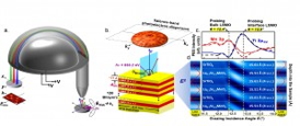 |
| Experimental setup and basic principles of SWARPES shows (a) the experimental setup; (b) diagram of the multilayer STO and LSMO film; (c) SW-excited photoemission intensity rocking curves and (d) simulated intensity of the x-ray standing wave field as a function of depth and grazing incidence angle. |
Abstract:
"The interface is the device," Nobel laureate Herbert Kroemer famously observed, referring to the remarkable properties to be found at the junctures where layers of different materials meet. In today's burgeoning world of nanotechnology, the interfaces between layers of metal oxides are becoming increasingly prominent, with applications in such high-tech favorites as spintronics, high-temperature superconductors, ferroelectrics and multiferroics. Realizing the vast potential of these metal oxide interfaces, especially those buried in subsurface layers, will require detailed knowledge of their electronic structure.
A Deeper Look at Interfaces: Researchers at Berkeley Lab’s Advanced Light Source Develop New Technique for Probing Subsurface Electronic Structure
Berkeley, CA | Posted on January 15th, 2014A new technique from an international team of researchers working at Berkeley Lab's Advanced Light Source (ALS) promises to deliver the goods. In a study led by Charles Fadley, a physicist who holds joint appointments with Berkeley Lab's Materials Sciences Division and the University of California Davis, where he is a Distinguished Professor of Physics, the team combined two well-established techniques for studying electronic structure in crystalline materials into a new technique that is optimized for examining electronic properties at subsurface interfaces. They call this new technique SWARPES, for Standing Wave Angle-Resolved Photoemission Spectroscopy.
"SWARPES allows us for the first time to selectively study buried interfaces with either soft or hard x-rays," Fadley says. "The technique can be applied to any multilayer prototype device structure in spintronics, strongly correlated/high-TC superconductors, or semiconductor electronics. The only limitations are that the sample has to have a high degree of crystalline order, and has to be grown on a nanoscale multilayer mirror suitable for generating an x-ray standing wave."
As the name indicates, SWARPES combines the use of standing waves of x-rays with ARPES, the technique of choice for studying electronic structure. A standing wave is a vibrational pattern created when two waves of identical wavelength interfere with one another: one is the incident x-ray and the other is the x-ray reflected by a mirror. Interactions between standing waves and core-level electrons reveal much about the properties of each atomic species in a sample. ARPES from the outer valence levels is the long-standing spectroscopic workhorse for the study of electronic structure. X-rays striking a material surface or interface cause the photoemission of electrons at angles and kinetic energies that can be measured to obtain detailed electronic energy levels of the sample. While an extremely powerful tool, ARPES, a soft x-ray technique, is primarily limited to the study of near-surface atoms. It's harder x-ray cousin, HARPES, makes use of more energetic x-rays to effectively probe subsurface interfaces, but the addition of the standing wave capability provides a much desired depth selectivity.
"The standing wave can be moved up and down in a sample simply by rocking the angle of incidence around the Bragg angle of the mirror," says Alexander Gray, a former member of Fadley's UC Davis research group and affiliate with Berkeley Lab's Materials Sciences Division, who is now a postdoctoral associate at Stanford/SLAC. "Observing an interface between a ferromagnetic conductor (lanthanum strontium manganite) and an insulator (strontium titanate), which constitute a magnetic tunnel junction used in spintronic logic circuits, we've shown that changes in the electronic structure can be reliably measured, and that these changes are semi-quantitatively predicted by theory at several levels. Our results point to a much wider use of SWARPES in the future for studying the electronic properties of buried interfaces of many different kinds."
Fadley, Gray and their collaborators carried out their SWARPES tests at ALS Beamline 7.0.1. The Advanced Light Source is a U.S. Department of Energy (DOE) national user facility and Beamline 7.0.1 features a premier endstation for determining the electronic structure of metals, semiconductors and insulators. Additional corroborating measurements concerning the interface atomic structure were performed at the National Center for Electron Microscopy (NCEM), another DOE national user facility hosted at Berkeley Lab.
This research was supported primarily by the U.S. Department of Energy (DOE) Office of Science.
####
For more information, please click here
Contacts:
Lynn Yarris
510-486-5375
Copyright © Berkeley Lab
If you have a comment, please Contact us.Issuers of news releases, not 7th Wave, Inc. or Nanotechnology Now, are solely responsible for the accuracy of the content.
Bookmark:


| Related Links |
![]() For more about the research of Charles Fadley, go here:
For more about the research of Charles Fadley, go here:
![]() For more about Berkeley Lab’s Advanced Light Source go here:
For more about Berkeley Lab’s Advanced Light Source go here:
| Related News Press |
News and information
![]() Simulating magnetization in a Heisenberg quantum spin chain April 5th, 2024
Simulating magnetization in a Heisenberg quantum spin chain April 5th, 2024
![]() NRL charters Navy’s quantum inertial navigation path to reduce drift April 5th, 2024
NRL charters Navy’s quantum inertial navigation path to reduce drift April 5th, 2024
![]() Discovery points path to flash-like memory for storing qubits: Rice find could hasten development of nonvolatile quantum memory April 5th, 2024
Discovery points path to flash-like memory for storing qubits: Rice find could hasten development of nonvolatile quantum memory April 5th, 2024
Superconductivity
![]() Optically trapped quantum droplets of light can bind together to form macroscopic complexes March 8th, 2024
Optically trapped quantum droplets of light can bind together to form macroscopic complexes March 8th, 2024
![]() 'Sudden death' of quantum fluctuations defies current theories of superconductivity: Study challenges the conventional wisdom of superconducting quantum transitions January 12th, 2024
'Sudden death' of quantum fluctuations defies current theories of superconductivity: Study challenges the conventional wisdom of superconducting quantum transitions January 12th, 2024
![]() Researchers at Purdue discover superconductive images are actually 3D and disorder-driven fractals May 12th, 2023
Researchers at Purdue discover superconductive images are actually 3D and disorder-driven fractals May 12th, 2023
Govt.-Legislation/Regulation/Funding/Policy
![]() NRL charters Navy’s quantum inertial navigation path to reduce drift April 5th, 2024
NRL charters Navy’s quantum inertial navigation path to reduce drift April 5th, 2024
![]() Discovery points path to flash-like memory for storing qubits: Rice find could hasten development of nonvolatile quantum memory April 5th, 2024
Discovery points path to flash-like memory for storing qubits: Rice find could hasten development of nonvolatile quantum memory April 5th, 2024
![]() Chemical reactions can scramble quantum information as well as black holes April 5th, 2024
Chemical reactions can scramble quantum information as well as black holes April 5th, 2024
Spintronics
![]() Quantum materials: Electron spin measured for the first time June 9th, 2023
Quantum materials: Electron spin measured for the first time June 9th, 2023
![]() Linearly assembled Ag-Cu nanoclusters: Spin transfer and distance-dependent spin coupling November 4th, 2022
Linearly assembled Ag-Cu nanoclusters: Spin transfer and distance-dependent spin coupling November 4th, 2022
Chip Technology
![]() Discovery points path to flash-like memory for storing qubits: Rice find could hasten development of nonvolatile quantum memory April 5th, 2024
Discovery points path to flash-like memory for storing qubits: Rice find could hasten development of nonvolatile quantum memory April 5th, 2024
![]() Utilizing palladium for addressing contact issues of buried oxide thin film transistors April 5th, 2024
Utilizing palladium for addressing contact issues of buried oxide thin film transistors April 5th, 2024
![]() HKUST researchers develop new integration technique for efficient coupling of III-V and silicon February 16th, 2024
HKUST researchers develop new integration technique for efficient coupling of III-V and silicon February 16th, 2024
Discoveries
![]() Chemical reactions can scramble quantum information as well as black holes April 5th, 2024
Chemical reactions can scramble quantum information as well as black holes April 5th, 2024
![]() New micromaterial releases nanoparticles that selectively destroy cancer cells April 5th, 2024
New micromaterial releases nanoparticles that selectively destroy cancer cells April 5th, 2024
![]() Utilizing palladium for addressing contact issues of buried oxide thin film transistors April 5th, 2024
Utilizing palladium for addressing contact issues of buried oxide thin film transistors April 5th, 2024
Materials/Metamaterials/Magnetoresistance
![]() Nanoscale CL thermometry with lanthanide-doped heavy-metal oxide in TEM March 8th, 2024
Nanoscale CL thermometry with lanthanide-doped heavy-metal oxide in TEM March 8th, 2024
![]() Focused ion beam technology: A single tool for a wide range of applications January 12th, 2024
Focused ion beam technology: A single tool for a wide range of applications January 12th, 2024
Announcements
![]() NRL charters Navy’s quantum inertial navigation path to reduce drift April 5th, 2024
NRL charters Navy’s quantum inertial navigation path to reduce drift April 5th, 2024
![]() Discovery points path to flash-like memory for storing qubits: Rice find could hasten development of nonvolatile quantum memory April 5th, 2024
Discovery points path to flash-like memory for storing qubits: Rice find could hasten development of nonvolatile quantum memory April 5th, 2024
Interviews/Book Reviews/Essays/Reports/Podcasts/Journals/White papers/Posters
![]() Simulating magnetization in a Heisenberg quantum spin chain April 5th, 2024
Simulating magnetization in a Heisenberg quantum spin chain April 5th, 2024
![]() Discovery points path to flash-like memory for storing qubits: Rice find could hasten development of nonvolatile quantum memory April 5th, 2024
Discovery points path to flash-like memory for storing qubits: Rice find could hasten development of nonvolatile quantum memory April 5th, 2024
Tools
![]() Ferroelectrically modulate the Fermi level of graphene oxide to enhance SERS response November 3rd, 2023
Ferroelectrically modulate the Fermi level of graphene oxide to enhance SERS response November 3rd, 2023
![]() The USTC realizes In situ electron paramagnetic resonance spectroscopy using single nanodiamond sensors November 3rd, 2023
The USTC realizes In situ electron paramagnetic resonance spectroscopy using single nanodiamond sensors November 3rd, 2023
|
|
||
|
|
||
| The latest news from around the world, FREE | ||
|
|
||
|
|
||
| Premium Products | ||
|
|
||
|
Only the news you want to read!
Learn More |
||
|
|
||
|
Full-service, expert consulting
Learn More |
||
|
|
||