Home > Press > Taking a New Look at Carbon Nanotubes: Berkeley Researchers Develop Technique For Imaging Individual Carbon Nanotubes
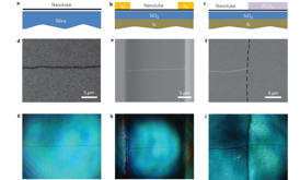 |
| In this display showing optical imaging and spectroscopy of an individual nanotube on substrates and in devices, (a�c) are schematics of a nanotube on a fused-silica substrate, in a field-effect transistor device with two gold electrodes, and under an alumina dielectric layer; (d�f) are SEM images and (g-i) are direct optical images of these individual nanotubes. |
Abstract:
Despite their almost incomprehensibly small size - a diameter about one ten-thousandth the thickness of a human hair - single-walled carbon nanotubes come in a plethora of different "species," each with its own structure and unique combination of electronic and optical properties. Characterizing the structure and properties of an individual carbon nanotube has involved a lot of guesswork - until now.
Taking a New Look at Carbon Nanotubes: Berkeley Researchers Develop Technique For Imaging Individual Carbon Nanotubes
Berkeley, CA | Posted on November 12th, 2013Researchers with the U.S. Department of Energy (DOE)'s Lawrence Berkeley National Laboratory (Berkeley Lab) and the University of California (UC) Berkeley have developed a technique that can be used to identify the structure of an individual carbon nanotube and characterize its electronic and optical properties in a functional device.
"Using a novel high-contrast polarization-based optical microscopy set-up, we've demonstrated video-rate imaging and in-situ spectroscopy of individual carbon nanotubes on various substrates and in functional devices," says Feng Wang, a condensed matter physicist with Berkeley Lab's Materials Sciences Division. "For the first time, we can take images and spectra of individual nanotubes in a general environment, including on substrates or in functional devices, which should be a great tool for advancing nanotube technology."
Wang, who is also a professor with UC Berkeley's Physics Department, is the corresponding author of a paper describing this research in the journal Nature Nanotechnology. The paper is titled "High-throughput optical imaging and spectroscopy of individual carbon nanotubes in devices." Co-authors are Kaihui Liu, Xiaoping Hong, Qin Zhou, Chenhao Jin, Jinghua Li, Weiwei Zhou, Jie Liu, Enge Wang and Alex Zettl.
A single-walled carbon nanotube can be metallic or semiconducting depending on its exact structure. Semiconducting nanotubes can have very different electronic bandgaps, resulting in wildly different electronic or optical properties.
"To fully understand field-effect devices or optoelectronic devices made from single-walled carbon nanotubes, it is critical to know what species of carbon nanotube is in the device," Wang says. "In the past, such information could not be obtained and researchers had to guess as to what was going on."
The physical structure and electronic properties of each individual species of single-walled carbon nanotubes are governed by chirality, meaning their structure has a distinct left/right orientation or "handedness," which cannot be superimposed on a mirror image. As a result, achieving chirality-controlled growth of carbon nanotubes and understanding the physics behind chirality-dependent devices are two of the biggest challenges in nanotube research.
"Polarization-based optical microscopy and spectroscopy techniques are well-suited for meeting these challenges, as polarized light is extremely sensitive to optical anisotropy in a system and has long been exploited to study chirality in molecules and crystals," Wang says. "However, the small signal and unavoidable environment background has made it difficult to use polarized optical microscopy to study single carbon nanotubes."
Difficulties arise from an apparent contradiction in polarization-based optical microscopy. For any optical microscope, a large numerical aperture (NA) objective is crucial for high-spatial resolution, but polarized light passing through a large NA objective becomes strongly depolarized. With their new technique, Wang and his colleagues were able to do what has not been done before and simultaneously achieve both high polarization and high spatial resolution.
"The key to our success was the realization that light illumination and light collection can be controlled separately," Wang says. "We used a large NA objective for light collection to obtain high spatial resolution, but were able to create an effectively small NA objective for illumination to maintain high polarization purity."
In their set-up, Wang and his colleagues collected nanotube-scattered polarized light with a 0.8 NA objective but used a much more narrow incident beam to create illumination light from a supercontinuum laser with a much smaller NA. The result was polarization an order of magnitude higher than what has been achieved with conventional polarized microscopy and spatial resolution at the nanoscale. This enabled them to obtain complete chirality profiles of hundreds of as-grown carbon nanotubes, and to perform in-situ monitoring in active field-effect devices.
"We observed that high order nanotube optical resonances are dramatically broadened by electrostatic doping, an unexpected behavior that points to strong inter-band electron-electron scattering processes dominating the ultrafast dynamics of excited states in carbon nanotubes," Wang says.
In addition to individual single-walled carbon nanotubes, Wang and his colleagues say their technique can also be used to greatly enhance the optical contrast of other anisotropic nano-sized materials that are "invisible" to conventional optical microscopes, including graphene nanoribbons, semiconductor nanowires and nanorods, and nanobiomaterials such as actin filaments.
This research was supported by grants from the National Science Foundation, the Center for Integrated Nanomechanical Systems, and by DOE's Office of Science.
####
About Berkeley Lab
Lawrence Berkeley National Laboratory (Berkeley Lab) addresses the world�s most urgent scientific challenges by advancing sustainable energy, protecting human health, creating new materials, and revealing the origin and fate of the universe. Founded in 1931, Berkeley Lab�s scientific expertise has been recognized with 13 Nobel prizes. The University of California manages Berkeley Lab for the U.S. Department of Energy�s Office of Science. For more, visit www.lbl.gov.
DOE�s Office of Science is the single largest supporter of basic research in the physical sciences in the United States, and is working to address some of the most pressing challenges of our time. For more information, please visit the Office of Science website at science.energy.gov.
For more information, please click here
Contacts:
Lynn Yarris
510-486-5375
Copyright © Berkeley Lab
If you have a comment, please Contact us.Issuers of news releases, not 7th Wave, Inc. or Nanotechnology Now, are solely responsible for the accuracy of the content.
Bookmark:


| Related Links |
![]() For more about the research of Feng Wang go here:
For more about the research of Feng Wang go here:
| Related News Press |
News and information
![]() Simulating magnetization in a Heisenberg quantum spin chain April 5th, 2024
Simulating magnetization in a Heisenberg quantum spin chain April 5th, 2024
![]() NRL charters Navy�s quantum inertial navigation path to reduce drift April 5th, 2024
NRL charters Navy�s quantum inertial navigation path to reduce drift April 5th, 2024
![]() Discovery points path to flash-like memory for storing qubits: Rice find could hasten development of nonvolatile quantum memory April 5th, 2024
Discovery points path to flash-like memory for storing qubits: Rice find could hasten development of nonvolatile quantum memory April 5th, 2024
Imaging
![]() Nanoscale CL thermometry with lanthanide-doped heavy-metal oxide in TEM March 8th, 2024
Nanoscale CL thermometry with lanthanide-doped heavy-metal oxide in TEM March 8th, 2024
Laboratories
![]() A battery�s hopping ions remember where they�ve been: Seen in atomic detail, the seemingly smooth flow of ions through a battery�s electrolyte is surprisingly complicated February 16th, 2024
A battery�s hopping ions remember where they�ve been: Seen in atomic detail, the seemingly smooth flow of ions through a battery�s electrolyte is surprisingly complicated February 16th, 2024
![]() NRL discovers two-dimensional waveguides February 16th, 2024
NRL discovers two-dimensional waveguides February 16th, 2024
Govt.-Legislation/Regulation/Funding/Policy
![]() NRL charters Navy�s quantum inertial navigation path to reduce drift April 5th, 2024
NRL charters Navy�s quantum inertial navigation path to reduce drift April 5th, 2024
![]() Discovery points path to flash-like memory for storing qubits: Rice find could hasten development of nonvolatile quantum memory April 5th, 2024
Discovery points path to flash-like memory for storing qubits: Rice find could hasten development of nonvolatile quantum memory April 5th, 2024
![]() Chemical reactions can scramble quantum information as well as black holes April 5th, 2024
Chemical reactions can scramble quantum information as well as black holes April 5th, 2024
Nanotubes/Buckyballs/Fullerenes/Nanorods/Nanostrings
![]() Tests find no free-standing nanotubes released from tire tread wear September 8th, 2023
Tests find no free-standing nanotubes released from tire tread wear September 8th, 2023
![]() Detection of bacteria and viruses with fluorescent nanotubes July 21st, 2023
Detection of bacteria and viruses with fluorescent nanotubes July 21st, 2023
Discoveries
![]() Chemical reactions can scramble quantum information as well as black holes April 5th, 2024
Chemical reactions can scramble quantum information as well as black holes April 5th, 2024
![]() New micromaterial releases nanoparticles that selectively destroy cancer cells April 5th, 2024
New micromaterial releases nanoparticles that selectively destroy cancer cells April 5th, 2024
![]() Utilizing palladium for addressing contact issues of buried oxide thin film transistors April 5th, 2024
Utilizing palladium for addressing contact issues of buried oxide thin film transistors April 5th, 2024
Announcements
![]() NRL charters Navy�s quantum inertial navigation path to reduce drift April 5th, 2024
NRL charters Navy�s quantum inertial navigation path to reduce drift April 5th, 2024
![]() Discovery points path to flash-like memory for storing qubits: Rice find could hasten development of nonvolatile quantum memory April 5th, 2024
Discovery points path to flash-like memory for storing qubits: Rice find could hasten development of nonvolatile quantum memory April 5th, 2024
Interviews/Book Reviews/Essays/Reports/Podcasts/Journals/White papers/Posters
![]() Simulating magnetization in a Heisenberg quantum spin chain April 5th, 2024
Simulating magnetization in a Heisenberg quantum spin chain April 5th, 2024
![]() Discovery points path to flash-like memory for storing qubits: Rice find could hasten development of nonvolatile quantum memory April 5th, 2024
Discovery points path to flash-like memory for storing qubits: Rice find could hasten development of nonvolatile quantum memory April 5th, 2024
Tools
![]() Ferroelectrically modulate the Fermi level of graphene oxide to enhance SERS response November 3rd, 2023
Ferroelectrically modulate the Fermi level of graphene oxide to enhance SERS response November 3rd, 2023
![]() The USTC realizes In situ electron paramagnetic resonance spectroscopy using single nanodiamond sensors November 3rd, 2023
The USTC realizes In situ electron paramagnetic resonance spectroscopy using single nanodiamond sensors November 3rd, 2023
|
|
||
|
|
||
| The latest news from around the world, FREE | ||
|
|
||
|
|
||
| Premium Products | ||
|
|
||
|
Only the news you want to read!
Learn More |
||
|
|
||
|
Full-service, expert consulting
Learn More |
||
|
|
||