Home > Press > Columbia Engineers Develop New Device Architecture for 2D Materials, Making Electrical Contact from the 1D Edge: New Approach Produces Cleanest Graphene Yet, with Previously Unrealized Performance
 |
Abstract:
Columbia Engineering researchers have experimentally demonstrated for the first time that it is possible to electrically contact an atomically thin two-dimensional (2D) material only along its one-dimensional (1D) edge, rather than contacting it from the top, which has been the conventional approach. With this new contact architecture, they have developed a new assembly technique for layered materials that prevents contamination at the interfaces, and, using graphene as the model 2D material, show that these two methods in combination result in the cleanest graphene yet realized. The study is published in Science on November 1, 2013.
Columbia Engineers Develop New Device Architecture for 2D Materials, Making Electrical Contact from the 1D Edge: New Approach Produces Cleanest Graphene Yet, with Previously Unrealized Performance
New York, NY | Posted on October 31st, 2013 "This is an exciting new paradigm in materials engineering where instead of the conventional approach of layer by layer growth, hybrid materials can now be fabricated by mechanical assembly of constituent 2D crystals," says Electrical Engineering Professor Ken Shepard, co-author of the paper. "No other group has been able to successfully achieve a pure edge-contact geometry to 2D materials such as graphene."
He adds that earlier efforts have looked at how to improve �top contacts' by additional engineering such as adding dopants: "Our novel edge-contact geometry provides more efficient contact than the conventional geometry without the need for further complex processing. There are now many more possibilities in the pursuit of both device applications and fundamental physics explorations."
First isolated in 2004, graphene is the best-studied 2D material and has been the subject of thousands of papers studying its electrical behavior and device applications. "But in nearly all of this work, the performance of graphene is degraded by exposure to contamination," notes Mechanical Engineering Professor James Hone who is also a co-author of the study. "It turns out that the problems of contamination and electrical contact are linked. Any high-performance electronic material must be encapsulated in an insulator to protect it from the environment. Graphene lacks the ability to make out-of-plane bonds, which makes electrical contact through its surface difficult, but also prevents bonding to conventional 3D insulators such as oxides. Instead, the best results are obtained by using a 2D insulator, which does not need to make bonds at its surface. However, there has been no way to electrically access a fully-encapsulated graphene sheet until now."
In this work, says Cory Dean, who led the research as a postdoc at Columbia and is now an assistant professor at The City College of New York, the team solved both the contact and contamination problems at once. "One of the greatest assets of 2D materials such as graphene is that being only one atom thick, we have direct access to its electronic properties. At the same time, this can be one of its worst features since this makes the material extremely sensitive to its environment. Any external contamination quickly degrades performance. The need to protect graphene from unwanted disorder, while still allowing electrical access, has been the most significant roadblock preventing development of graphene-based technologies. By making contact only to the 1D edge of graphene, we have developed a fundamentally new way to bridge our 3D world to this fascinating 2D world, without disturbing its inherent properties. This virtually eliminates external contamination and finally allows graphene to show its true potential in electronic devices."
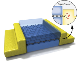
The researchers fully encapsulated the 2D graphene layer in a sandwich of thin insulating boron nitride crystals, employing a new technique in which crystal layers are stacked one-by-one. "Our approach for assembling these heterostructures completely eliminates any contamination between layers," Dean explains, "which we confirmed by cross-sectioning the devices and imaging them in a transmission electron microscope with atomic resolution."
Once they created the stack, they etched it to expose the edge of the graphene layer, and then evaporated metal onto the edge to create the electrical contact. By making contact along the edge, the team realized a 1D interface between the 2D active layer and 3D metal electrode. And, even though electrons entered only at the 1D atomic edge of the graphene sheet, the contact resistance was remarkably low, reaching 100 Ohms per micron of contact width�a value smaller than what can be achieved for contacts at the graphene top surface.
With the two new techniques�the contact architecture through the 1D edge and the stacking assembly method that prevents contamination at the interfaces�the team was able to produce what they say is the "cleanest graphene yet realized." At room temperature, these devices exhibit previously unachievable performance, including electron mobility at least twice as large as any conventional 2D electron system, and sheet resistivity less than 40 Ohms when sufficient charges are added to the sheet by electrostatic "gating." Amazingly, this 2D sheet resistance corresponds to a "bulk" 3D resistivity smaller than that of any metal at room temperature. At low temperature, electrons travel through the team's samples without scattering, a phenomenon known as ballistic transport. Ballistic transport, had previously been observed in samples close to one micrometer in size, but this work demonstrates the same behavior in samples as large as 20 micrometers. "So far this is limited purely by device size," says Dean, "indicating that the true �intrinsic' behavior is even better."
The team is now working on applying these techniques to develop new hybrid materials by mechanical assembly and edge contact of hybrid materials drawing from the full suite of available 2D layered materials, including graphene, boron nitride, transition metal dichlcogenides (TMDCs), transition metal oxides (TMOs), and topological insulators (TIs). "We are taking advantage of the unprecedented performance we now routinely achieve in graphene-based devices to explore effects and applications related to ballistic electron transport over fantastically large length scales," Dean adds. "With so much current research focused on developing new devices by integrating layered 2D systems, potential applications are incredible, from vertically structured transistors, tunneling based devices and sensors, photoactive hybrid materials, to flexible and transparent electronics."
"This work results from a wide collaboration of researchers interested in both pure and applied science," says Hone. "The unique environment at Columbia provides an unparalleled opportunity for these two communities to interact and build off one another."
The Columbia team demonstrated the first technique to mechanically layer 2D materials in 2010. These two new techniques, which are critical advancements in the field, are the result of interdisciplinary efforts by Lei Wang (PhD student, Electrical Engineering, Hone group) and Inanc Meric (Postdoc, Electrical Engineering, Shepard group), co-lead authors on this project who worked with the groups of Philip Kim (Physics and Applied Physics and Applied Mathematics, Columbia), James Hone (Mechanical Engineering, Columbia), Ken Shepard (Electrical Engineering, Columbia) and Cory Dean (Physics, City College of New York).
This work is supported by the Department of Defense (DoD) through the National Defense Science and Engineering Graduate Fellowship (NDSEG) Program, the National Science Foundation (DMR-1124894), the Air Force Office of Scientific Research (FA9550-09-1-0705), the office of Naval Research (N000141310662), the ONR Grant N000141110633 and the Defense Advanced Research Projects Agency (under ONR Grant N000141210814), and the Nano Material Technology Development Program through the National Research Foundation of Korea (2012M3A7B4049966).
####
About Columbia Engineering
Columbia University's Fu Foundation School of Engineering and Applied Science, founded in 1864, offers programs in nine departments to both undergraduate and graduate students. With facilities specifically designed and equipped to meet the laboratory and research needs of faculty and students, Columbia Engineering is home to NSF-NIH funded centers in genomic science, molecular nanostructures, materials science, and energy, as well as one of the world�s leading programs in financial engineering. These interdisciplinary centers are leading the way in their respective fields while individual groups of engineers and scientists collaborate to solve some of modern society�s more difficult challenges.
For more information, please click here
Contacts:
Holly Evarts
Director
Strategic Communications and Media Relations
212-854-3206 (o)
347-453-7408 (c)
Issuers of news releases, not 7th Wave, Inc. or Nanotechnology Now, are solely responsible for the accuracy of the content.
Bookmark:


| Related News Press |
News and information
![]() Simulating magnetization in a Heisenberg quantum spin chain April 5th, 2024
Simulating magnetization in a Heisenberg quantum spin chain April 5th, 2024
![]() NRL charters Navy�s quantum inertial navigation path to reduce drift April 5th, 2024
NRL charters Navy�s quantum inertial navigation path to reduce drift April 5th, 2024
![]() Discovery points path to flash-like memory for storing qubits: Rice find could hasten development of nonvolatile quantum memory April 5th, 2024
Discovery points path to flash-like memory for storing qubits: Rice find could hasten development of nonvolatile quantum memory April 5th, 2024
Graphene/ Graphite
![]() NRL discovers two-dimensional waveguides February 16th, 2024
NRL discovers two-dimensional waveguides February 16th, 2024
Govt.-Legislation/Regulation/Funding/Policy
![]() NRL charters Navy�s quantum inertial navigation path to reduce drift April 5th, 2024
NRL charters Navy�s quantum inertial navigation path to reduce drift April 5th, 2024
![]() Discovery points path to flash-like memory for storing qubits: Rice find could hasten development of nonvolatile quantum memory April 5th, 2024
Discovery points path to flash-like memory for storing qubits: Rice find could hasten development of nonvolatile quantum memory April 5th, 2024
![]() Chemical reactions can scramble quantum information as well as black holes April 5th, 2024
Chemical reactions can scramble quantum information as well as black holes April 5th, 2024
Chip Technology
![]() Discovery points path to flash-like memory for storing qubits: Rice find could hasten development of nonvolatile quantum memory April 5th, 2024
Discovery points path to flash-like memory for storing qubits: Rice find could hasten development of nonvolatile quantum memory April 5th, 2024
![]() Utilizing palladium for addressing contact issues of buried oxide thin film transistors April 5th, 2024
Utilizing palladium for addressing contact issues of buried oxide thin film transistors April 5th, 2024
![]() HKUST researchers develop new integration technique for efficient coupling of III-V and silicon February 16th, 2024
HKUST researchers develop new integration technique for efficient coupling of III-V and silicon February 16th, 2024
Nanoelectronics
![]() Interdisciplinary: Rice team tackles the future of semiconductors Multiferroics could be the key to ultralow-energy computing October 6th, 2023
Interdisciplinary: Rice team tackles the future of semiconductors Multiferroics could be the key to ultralow-energy computing October 6th, 2023
![]() Key element for a scalable quantum computer: Physicists from Forschungszentrum J�lich and RWTH Aachen University demonstrate electron transport on a quantum chip September 23rd, 2022
Key element for a scalable quantum computer: Physicists from Forschungszentrum J�lich and RWTH Aachen University demonstrate electron transport on a quantum chip September 23rd, 2022
![]() Reduced power consumption in semiconductor devices September 23rd, 2022
Reduced power consumption in semiconductor devices September 23rd, 2022
![]() Atomic level deposition to extend Moore�s law and beyond July 15th, 2022
Atomic level deposition to extend Moore�s law and beyond July 15th, 2022
Discoveries
![]() Chemical reactions can scramble quantum information as well as black holes April 5th, 2024
Chemical reactions can scramble quantum information as well as black holes April 5th, 2024
![]() New micromaterial releases nanoparticles that selectively destroy cancer cells April 5th, 2024
New micromaterial releases nanoparticles that selectively destroy cancer cells April 5th, 2024
![]() Utilizing palladium for addressing contact issues of buried oxide thin film transistors April 5th, 2024
Utilizing palladium for addressing contact issues of buried oxide thin film transistors April 5th, 2024
Announcements
![]() NRL charters Navy�s quantum inertial navigation path to reduce drift April 5th, 2024
NRL charters Navy�s quantum inertial navigation path to reduce drift April 5th, 2024
![]() Discovery points path to flash-like memory for storing qubits: Rice find could hasten development of nonvolatile quantum memory April 5th, 2024
Discovery points path to flash-like memory for storing qubits: Rice find could hasten development of nonvolatile quantum memory April 5th, 2024
Military
![]() NRL charters Navy�s quantum inertial navigation path to reduce drift April 5th, 2024
NRL charters Navy�s quantum inertial navigation path to reduce drift April 5th, 2024
![]() What heat can tell us about battery chemistry: using the Peltier effect to study lithium-ion cells March 8th, 2024
What heat can tell us about battery chemistry: using the Peltier effect to study lithium-ion cells March 8th, 2024
![]() New chip opens door to AI computing at light speed February 16th, 2024
New chip opens door to AI computing at light speed February 16th, 2024
Grants/Sponsored Research/Awards/Scholarships/Gifts/Contests/Honors/Records
![]() Discovery points path to flash-like memory for storing qubits: Rice find could hasten development of nonvolatile quantum memory April 5th, 2024
Discovery points path to flash-like memory for storing qubits: Rice find could hasten development of nonvolatile quantum memory April 5th, 2024
![]() Chemical reactions can scramble quantum information as well as black holes April 5th, 2024
Chemical reactions can scramble quantum information as well as black holes April 5th, 2024
Research partnerships
![]() Discovery points path to flash-like memory for storing qubits: Rice find could hasten development of nonvolatile quantum memory April 5th, 2024
Discovery points path to flash-like memory for storing qubits: Rice find could hasten development of nonvolatile quantum memory April 5th, 2024
![]() Researchers� approach may protect quantum computers from attacks March 8th, 2024
Researchers� approach may protect quantum computers from attacks March 8th, 2024
![]() 'Sudden death' of quantum fluctuations defies current theories of superconductivity: Study challenges the conventional wisdom of superconducting quantum transitions January 12th, 2024
'Sudden death' of quantum fluctuations defies current theories of superconductivity: Study challenges the conventional wisdom of superconducting quantum transitions January 12th, 2024
|
|
||
|
|
||
| The latest news from around the world, FREE | ||
|
|
||
|
|
||
| Premium Products | ||
|
|
||
|
Only the news you want to read!
Learn More |
||
|
|
||
|
Full-service, expert consulting
Learn More |
||
|
|
||