Home > Press > FEI Revolutionizes the World of TEM with the Introduction of Three New Systems: The new TEM systems continue FEI’s emphasis on technology leadership while redefining its product portfolio for efficient and effective application-specific workflows
 |
Abstract:
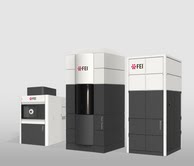
FEI (NASDAQ: FEIC) today introduced three new systems that tailor the power of transmission electron microscopy (TEM) to specific application and industry needs. The new systems launched today provide efficient and effective application-specific workflows for semiconductor manufacturing and scientific research. They include the new Metrios™ TEM for advanced semiconductor manufacturing metrology, Talos™ TEM that provides high-speed imaging and analysis for materials and life sciences applications, and the Titan™ Themis™ TEM for enhanced atomic-scale measurements of material properties.
FEI Revolutionizes the World of TEM with the Introduction of Three New Systems: The new TEM systems continue FEI’s emphasis on technology leadership while redefining its product portfolio for efficient and effective application-specific workflows
Hillsboro, OR | Posted on August 1st, 2013"With these three systems we have now introduced an unprecedented total of six new TEMs in the past year," said Benjamin Loh, FEI's executive vice president and chief operating officer. "All six have been designed and built to provide an application-specific workflow that delivers contextual information of immediate value to users in science and industrial market segments, including: materials science, chemicals, life sciences, and semiconductor manufacturing. Our goal is to completely change the world of TEM so our customers can change their world as well."
The Metrios system is the first TEM dedicated to providing the fast, precise measurements that semiconductor manufacturers need to develop and control their wafer fabrication processes. Extensive automation of the basic TEM operation and measurement procedures minimizes requirements for specialized operator training. Its advanced automated metrology delivers greater precision than manual methods. The Metrios TEM is designed to provide customers with improved throughput and lower cost-per-sample than other TEMs.
The Talos TEM combines high-resolution, high-throughput TEM imaging with fast, precise and quantitative energy dispersive x-ray (EDX) analysis to deliver advanced analytical performance with class-leading value. The new TEM is available with FEI's highest brightness electron source and latest EDX detector technology to provide high-efficiency detection of low concentration and light elements, along with FEI's exclusive 3D EDS tomography. Excellent performance at lower accelerating voltages permits the use of lower beam energies to reduce sample damage on delicate materials. The Talos platform is completely digital, allowing for remote operation, and it also enables the addition of application-specific detectors or sample holders for dynamic experiments. With enhanced automation and ease-of-use, the Talos is especially well-suited for the individual investigator as well as multi-user laboratory environments.
The Titan Themis TEM extends FEI's leadership position in aberration-corrected, atomic-scale imaging and analysis. Researchers use the high resolution of aberration-corrected TEM to understand relationships between a material's larger-scale physical properties and its atomic-scale composition and structure. The Titan Themis platform enables direct measurements of properties, such as magnetic fields, on the nanometer-length scale and electric fields even down to the atomic scale. Automation of the complete TEM workflow, from sample navigation and alignment through final data acquisition, enhances the repeatability and reproducibility of results to enable more confident conclusions with less time and effort.
For more information about FEI's new suite of application-specific TEM workflows, please see http://www.fei.com/tembyfei/ , or visit FEI at the Microscopy & Microanalysis Conference, August 4-8, 2013, taking place in Indianapolis, IN, USA.
####
About FEI Company
FEI (Nasdaq: FEIC) is a leading supplier of scientific instruments for nanoscale applications and solutions for industry and science. With more than 60 years of technological innovation and leadership, FEI has set the performance standard in transmission electron microscopes (TEM), scanning electron microscopes (SEM) and DualBeams™, which combine a SEM with a focused ion beam (FIB). FEI has over 2,500 employees and sales and service operations in more than 50 countries around the world. More information can be found at: www.fei.com.
FEI Safe Harbor Statement
This news release contains forward-looking statements that include statements regarding the performance capabilities and benefits of the Metrios, Talos, and Titan Themis TEMs. Factors that could affect these forward-looking statements include but are not limited to failure of the product or technology to perform as expected and achieve anticipated results or cost savings, unexpected technology problems and challenges, changes to the technology, the inability of FEI, its suppliers or project partners to make the technological advances required for the technology to achieve anticipated results, the inability of customers to develop and deploy the expected new applications and our ability to manufacture, ship and deliver the tools or software as expected. Please also refer to our Form 10-K, Forms 10-Q, Forms 8-K and other filings with the U.S. Securities and Exchange Commission for additional information on these factors and other factors that could cause actual results to differ materially from the forward-looking statements. FEI assumes no duty to update forward-looking statements.
For more information, please click here
Contacts:
Sandy Fewkes
(media contact)
MindWrite Communications, Inc.
+1 408 224 4024
FEI Company
Fletcher Chamberlin
(investors and analysts
Investor Relations
+1 503 726 7710
Copyright © FEI Company
If you have a comment, please Contact us.Issuers of news releases, not 7th Wave, Inc. or Nanotechnology Now, are solely responsible for the accuracy of the content.
Bookmark:


| Related News Press |
News and information
![]() Simulating magnetization in a Heisenberg quantum spin chain April 5th, 2024
Simulating magnetization in a Heisenberg quantum spin chain April 5th, 2024
![]() NRL charters Navy’s quantum inertial navigation path to reduce drift April 5th, 2024
NRL charters Navy’s quantum inertial navigation path to reduce drift April 5th, 2024
![]() Discovery points path to flash-like memory for storing qubits: Rice find could hasten development of nonvolatile quantum memory April 5th, 2024
Discovery points path to flash-like memory for storing qubits: Rice find could hasten development of nonvolatile quantum memory April 5th, 2024
Imaging
![]() Nanoscale CL thermometry with lanthanide-doped heavy-metal oxide in TEM March 8th, 2024
Nanoscale CL thermometry with lanthanide-doped heavy-metal oxide in TEM March 8th, 2024
![]() The USTC realizes In situ electron paramagnetic resonance spectroscopy using single nanodiamond sensors November 3rd, 2023
The USTC realizes In situ electron paramagnetic resonance spectroscopy using single nanodiamond sensors November 3rd, 2023
![]() Observation of left and right at nanoscale with optical force October 6th, 2023
Observation of left and right at nanoscale with optical force October 6th, 2023
Announcements
![]() NRL charters Navy’s quantum inertial navigation path to reduce drift April 5th, 2024
NRL charters Navy’s quantum inertial navigation path to reduce drift April 5th, 2024
![]() Discovery points path to flash-like memory for storing qubits: Rice find could hasten development of nonvolatile quantum memory April 5th, 2024
Discovery points path to flash-like memory for storing qubits: Rice find could hasten development of nonvolatile quantum memory April 5th, 2024
Tools
![]() Ferroelectrically modulate the Fermi level of graphene oxide to enhance SERS response November 3rd, 2023
Ferroelectrically modulate the Fermi level of graphene oxide to enhance SERS response November 3rd, 2023
![]() The USTC realizes In situ electron paramagnetic resonance spectroscopy using single nanodiamond sensors November 3rd, 2023
The USTC realizes In situ electron paramagnetic resonance spectroscopy using single nanodiamond sensors November 3rd, 2023
Events/Classes
![]() Researchers demonstrate co-propagation of quantum and classical signals: Study shows that quantum encryption can be implemented in existing fiber networks January 20th, 2023
Researchers demonstrate co-propagation of quantum and classical signals: Study shows that quantum encryption can be implemented in existing fiber networks January 20th, 2023
|
|
||
|
|
||
| The latest news from around the world, FREE | ||
|
|
||
|
|
||
| Premium Products | ||
|
|
||
|
Only the news you want to read!
Learn More |
||
|
|
||
|
Full-service, expert consulting
Learn More |
||
|
|
||