Home > Press > Imec and Holst Centre Unveil Fully-Organic Imager
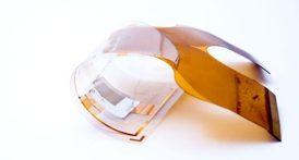 |
| Fully-organic, flexible imager developed by imec, Holst Centre and Philips Research |
Abstract:
At this week's International Image Sensor Workshop (IISW 2013, Snowbird, Utah, June 12-16 2013), imec and Holst Centre presented a large-area fully-organic photodetector array fabricated on a flexible substrate. The imager is sensitive in the wavelength range suitable for x-ray imaging applications.
Imec and Holst Centre Unveil Fully-Organic Imager
Leuven, Belgium | Posted on June 12th, 2013Because of their very high absorption coefficient, organic semiconductors allow extremely thin active layers (10 to 50 nm). Also, given their low processing temperature, they can be processed on foils. As a result, organic imagers can be more robust and light-weight compared to their traditional counterparts and may be used for conformal coating of randomly shaped substrates. Moreover, the wide variety of organic molecules available ensures that the properties of the active layer can be tuned to applications requiring specific wavelength ranges.
The presented imager is sensitive in the wavelength range between 500 and 600 nm, making it compatible with typical scintillators and therefore suitable for x-ray imaging applications. It was fabricated by thermally evaporating an ultrathin (submicron) photosensitive layer of small organic molecules (SubPc/C60) on top of an organic readout circuit. A semi-transparent top contact enables front-side illumination. The readout backplane was manufactured on six inch foil-laminated wafers. It consists of pentacene-based thin-film transistors (TFTs) in arrays of 32x32 pixels with varying pitch (1 mm and 200 �m). To prevent degradation of the organic semiconductors in the air, the photodetector array is encapsulated. The imager was characterized under illumination with a calibrated green light-emitting diode (LED), yielding a linearly increasing photocurrent from the incident power of 3 �W/cm2. Dark current density is below 10-6 A/cm2 at a bias voltage of -2V.
"This latest achievement is a significant step forward in not only finding the optimal materials, but pinpointing the best ways to process materials into reliable organic circuits and systems with state-of-the-art performance," said Paul Heremans, technology director at the imec/Holst Centre. "Once again, we're proud to demonstrate how imec's top-notch research leads to relevant industrial solutions, and subsequently brings added value to our partners' businesses."
This research results are presented in collaboration with Philips Research, at the (2013 International Image Sensor Workshop (IISW), sponsored by the International Image Sensor Society (IISS), June 12-16, 2013.
####
About IMEC
Imec performs world-leading research in nanoelectronics. Imec leverages its scientific knowledge with the innovative power of its global partnerships in ICT, healthcare and energy. Imec delivers industry-relevant technology solutions. In a unique high-tech environment, its international top talent is committed to providing the building blocks for a better life in a sustainable society. Imec is headquartered in Leuven, Belgium, and has offices in Belgium, the Netherlands, Taiwan, US, China, India and Japan. Its staff of more than 2,000 people includes more than 650 industrial residents and guest researchers. In 2012, imec's revenue (P&L) totaled 320 million euro. Further information on imec can be found at www.imec.be.
Imec is a registered trademark for the activities of IMEC International (a legal entity set up under Belgian law as a "stichting van openbaar nut�), imec Belgium (IMEC vzw supported by the Flemish Government), imec the Netherlands (Stichting IMEC Nederland, part of Holst Centre which is supported by the Dutch Government), imec Taiwan (IMEC Taiwan Co.) and imec China (IMEC Microelectronics (Shangai) Co. Ltd.) and imec India (Imec India Private Limited).
About Holst Centre
Holst Centre is an independent open-innovation R&D centre that develops generic technologies for Wireless Autonomous Transducer Solutions and for Systems-in-Foil. A key feature of Holst Centre is its partnership model with industry and academia around shared roadmaps and programs. It is this kind of cross-fertilization that enables Holst Centre to tune its scientific strategy to industrial needs.
Holst Centre was set up in 2005 by imec (Flanders, Belgium) and TNO (The Netherlands) with support from the Dutch Ministry of Economic Affairs and the Government of Flanders. It is named after Gilles Holst, a Dutch pioneer in Research and Development and first director of Philips Research.
Located on High Tech Campus Eindhoven, Holst Centre benefits from the state-of-the-art on-site facilities. Holst Centre has over 180 employees from around 28 nationalities and a commitment from more than 45 industrial partners.
Visit us at www.holstcentre.com
For more information, please click here
Contacts:
Imec :
Hanne Degans
External communications officer
T: +32 16 28 17 69
Mobile: +32 486 065 175
Holst Centre :
Koen Snoeckx
Communication Manager
T: +31 40 40 20 561
M: +31 612 71 98 43
Copyright © IMEC
If you have a comment, please Contact us.Issuers of news releases, not 7th Wave, Inc. or Nanotechnology Now, are solely responsible for the accuracy of the content.
Bookmark:


| Related News Press |
News and information
![]() Simulating magnetization in a Heisenberg quantum spin chain April 5th, 2024
Simulating magnetization in a Heisenberg quantum spin chain April 5th, 2024
![]() NRL charters Navy�s quantum inertial navigation path to reduce drift April 5th, 2024
NRL charters Navy�s quantum inertial navigation path to reduce drift April 5th, 2024
![]() Discovery points path to flash-like memory for storing qubits: Rice find could hasten development of nonvolatile quantum memory April 5th, 2024
Discovery points path to flash-like memory for storing qubits: Rice find could hasten development of nonvolatile quantum memory April 5th, 2024
Imaging
![]() Nanoscale CL thermometry with lanthanide-doped heavy-metal oxide in TEM March 8th, 2024
Nanoscale CL thermometry with lanthanide-doped heavy-metal oxide in TEM March 8th, 2024
![]() The USTC realizes In situ electron paramagnetic resonance spectroscopy using single nanodiamond sensors November 3rd, 2023
The USTC realizes In situ electron paramagnetic resonance spectroscopy using single nanodiamond sensors November 3rd, 2023
![]() Observation of left and right at nanoscale with optical force October 6th, 2023
Observation of left and right at nanoscale with optical force October 6th, 2023
Chip Technology
![]() Discovery points path to flash-like memory for storing qubits: Rice find could hasten development of nonvolatile quantum memory April 5th, 2024
Discovery points path to flash-like memory for storing qubits: Rice find could hasten development of nonvolatile quantum memory April 5th, 2024
![]() Utilizing palladium for addressing contact issues of buried oxide thin film transistors April 5th, 2024
Utilizing palladium for addressing contact issues of buried oxide thin film transistors April 5th, 2024
![]() HKUST researchers develop new integration technique for efficient coupling of III-V and silicon February 16th, 2024
HKUST researchers develop new integration technique for efficient coupling of III-V and silicon February 16th, 2024
Announcements
![]() NRL charters Navy�s quantum inertial navigation path to reduce drift April 5th, 2024
NRL charters Navy�s quantum inertial navigation path to reduce drift April 5th, 2024
![]() Discovery points path to flash-like memory for storing qubits: Rice find could hasten development of nonvolatile quantum memory April 5th, 2024
Discovery points path to flash-like memory for storing qubits: Rice find could hasten development of nonvolatile quantum memory April 5th, 2024
Tools
![]() Ferroelectrically modulate the Fermi level of graphene oxide to enhance SERS response November 3rd, 2023
Ferroelectrically modulate the Fermi level of graphene oxide to enhance SERS response November 3rd, 2023
![]() The USTC realizes In situ electron paramagnetic resonance spectroscopy using single nanodiamond sensors November 3rd, 2023
The USTC realizes In situ electron paramagnetic resonance spectroscopy using single nanodiamond sensors November 3rd, 2023
Events/Classes
![]() Researchers demonstrate co-propagation of quantum and classical signals: Study shows that quantum encryption can be implemented in existing fiber networks January 20th, 2023
Researchers demonstrate co-propagation of quantum and classical signals: Study shows that quantum encryption can be implemented in existing fiber networks January 20th, 2023
|
|
||
|
|
||
| The latest news from around the world, FREE | ||
|
|
||
|
|
||
| Premium Products | ||
|
|
||
|
Only the news you want to read!
Learn More |
||
|
|
||
|
Full-service, expert consulting
Learn More |
||
|
|
||