Home > Press > Silex Microsystems Joins ENIAC Project PROMINENT To Bring Flexible and Cost Effective Inkjet Technologies to the MEMS Manufacturing Process: Silex Will Develop New Solutions for Through-Silicon Via Manufacture and Hermetic Wafer Bonding
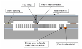 |
| Areas of process development under the ENIAC funded program PROMINENT |
Abstract:
Silex Microsystems, the world's largest pure-play MEMS foundry, today announced that it has joined an international European Union-funded program aimed at developing a new MEMS manufacturing platform based on advanced inkjet-based printing technologies. The program, "Processes for MEMS by Inkjet Enhanced Technologies," or PROMINENT, is leveraging the proven benefits of inkjet technologies to enable higher manufacturing efficiencies, increased product innovation, faster time-to-market, and lower costs throughout the entire MEMS manufacturing process. Silex's contributions in this effort will include new low-cost technologies for through-wafer vias, hermetic high-vacuum seals for wafer-to-wafer bonding including advanced material deposition, advances in piezo-MEMS fabrication, and other functional materials processing.
Silex Microsystems Joins ENIAC Project PROMINENT To Bring Flexible and Cost Effective Inkjet Technologies to the MEMS Manufacturing Process: Silex Will Develop New Solutions for Through-Silicon Via Manufacture and Hermetic Wafer Bonding
J�rf�lla, Sweden | Posted on May 13th, 2013As an innovation-driven industry, MEMS manufacturing depends on continuous innovation and exploitation of new technologies such as ink-jet processes. Ink-jet technology is one of the most mature MEMS technologies, having been in production since the late �70s and a mainstream of the digital printing industry since the early �80s. Similar to the impact that inkjet printing has had on the printing industry, the technology offers the promise of direct-to-wafer digitally-based patterning of wafer processing which can allow highly flexible prototyping and low-volume production for MEMS devices. In addition, advances in materials, electronics, and thin film compounds in recent years have opened up new avenues to apply ink-jet techniques to traditional manufacturing challenges such as metallization patterning using metallized inks. PROMINENT has been formed to exploit these new techniques and to advance the competitiveness of the European technology community.
"As a key partner in the PROMINENT project, Silex brings its extensive experience in metal TSVs and wafer bonding which will help end-users, partners in the consortium, and future customers advance the use of inkjet technologies for production purposes," says Dr. Thorbj�rn Ebefors, Chief Technologist at Silex Microsystems. "These new technologies have the potential to reduce costs and speed development time of new MEMS products, at no loss of performance for the customer."
"Printed electronics have recently achieved considerable progress due to new printing technologies and the introduction of nanoparticle inks, paving the way towards integrating these capabilities within silicon-based nanoelectronics," says Dr. Markku Tilli of Okmetic Oyj, PROMINENT project coordinator. "The objective of the ENIAC JU project PROMINENT is to demonstrate significant cost reduction in MEMS manufacturing by using printing technologies to reduce materials, chemicals and energy consumption, waste water production, processing cycle time and capital investments."
PROMINENT will develop novel low-cost, digitally controlled additive manufacturing methods that can radically change the manufacturing methods for MEMS and bring a substantial competitive edge to the European MEMS industry. The objective is not to replace the whole MEMS manufacturing process, but rather to introduce a new way of making its selected steps flow in a different, more flexible and cost-efficient way using methods developed in the printed electronics field.
By using maskless, digitally controlled, localized additive processes instead of the subtractive processes currently in use, selected steps in MEMS manufacturing can be done with a simplified process sequence. This will result in:
� Lower initial investment costs for a MEMS line, making it easier for manufacturers to introduce new products.
� New features in the MEMS devices, new application areas.
� Greatly increased flexibility in production, allowing for smaller batches, mass customization and fast changes in the production process.
� Increased flexibility, easier prototyping and shorter time-to-market for new MEMS devices.
� Greatly reduced production costs and environmental impact.
Technologies developed by Silex through PROMINENT will have direct applicability to the company's MEMS customers as well as the growing market for silicon interposers. Silex's ongoing work in PZT and AlN piezoelectric materials will also directly contribute to PROMINENT's projects.
####
About Silex Microsystems
As the world�s largest pure-play MEMS foundry, Silex Microsystems is driving the sensory system revolution by partnering with the world�s most innovative companies to commercialize MEMS technologies that are changing the world. Our unique expertise in providing cutting-edge MEMS foundry services, innovative process technologies and proven high volume production capabilities enable MEMS innovators to rapidly, cost-effectively and reliably commercialize and ramp products to high volume. At Silex, customers work closely with the industry�s most knowledgeable and creative MEMS manufacturing experts and benefit from our global ecosystem of development partners to take MEMS to market faster.
About PROMINENT
The multi-disciplinary ENIAC JU project Prominent requires expertise in different technology areas; ranging from MEMS research and wafer manufacturing, MEMS design and manufacturing to inkjet printing machinery and packaging . Thus, the consortium is built of a number of leading experts from universities, small and medium size companies, and large MEMS manufacturers, representing different value chain levels of the MEMS industry. The parties have complementary expertise in conception, design, evaluation and manufacturing of MEMS components, as well as ink, printing and surface treatment equipment development and manufacturing.
Silex Microsystems AB is one of the ten top-tier industrial and research partners from Finland, Norway, the Netherlands, Portugal, and Sweden forming the PROMINENT partnership. A total of �9.4M is to be spent on this program over 36 months, from a combination of ENIAC funds, a public-private partnership, member country national budgets, and the participating companies. Aside from Silex, PROMINENT members include Okmetic Oyj, Murata Electronics Oy, Tampere University of Technology, and Spinverse Oy, all from Finland; The Department of Micro and Nanosystems at KTH Royal Institute of Technology, and Micronic Mydata AB from Sweden; InnoPhysics BV from The Netherlands; poLight AS from Norway and Nanium SA from Portugal. For more information see www.prominent-mems.eu
PROMINENT is coordinated by Dr. Markku Tilli of Okmetic Oyj of Finland. Okmetic is the world�s leading supplier of silicon wafers for MEMS manufacturing and a leading silicon solutions provider for the manufacture of pressure sensors, accelerometers, actuators, silicon-based microphones and microfluidic and optical devices. For more information, see www.okmetic.com. The management part of the coordination is subcontracted from Spinverse Oy.
About ENIAC JU
ENIAC JU (European Technology Platform on Nanoelectronics Joint Undertaking), a public-private partnership between the European Commission, 21 European countries and various nanoelectronics actors funds 1.4 M� of PROMINENT budget. National public funding from the participating nations covers 2.5 M�, and the remainder comes from PROMINENT partners. For more information see www.eniac.eu
About VINNOVA
National funding for PROMINENT is provided in part by VINNOVA, the Swedish Governmental Agency for Innovation Systems. VINNOVA invests in research and strengthens Sweden�s innovative capacity for competitiveness, sustainable development and growth. VINNOVA�s efforts range from programs for R&D projects in small companies and at universities, to long-term development of strong research and innovation environments that attract R&D investment and expertise from around the world. For more information see www.vinnova.se/en
For more information, please click here
Contacts:
Silex Microsystems Public Relations:
Kelly Karr
Tanis Communications
+1 (408) 718-9350
Copyright © Silex Microsystems
If you have a comment, please Contact us.Issuers of news releases, not 7th Wave, Inc. or Nanotechnology Now, are solely responsible for the accuracy of the content.
Bookmark:


| Related News Press |
News and information
![]() Simulating magnetization in a Heisenberg quantum spin chain April 5th, 2024
Simulating magnetization in a Heisenberg quantum spin chain April 5th, 2024
![]() NRL charters Navy�s quantum inertial navigation path to reduce drift April 5th, 2024
NRL charters Navy�s quantum inertial navigation path to reduce drift April 5th, 2024
![]() Discovery points path to flash-like memory for storing qubits: Rice find could hasten development of nonvolatile quantum memory April 5th, 2024
Discovery points path to flash-like memory for storing qubits: Rice find could hasten development of nonvolatile quantum memory April 5th, 2024
Govt.-Legislation/Regulation/Funding/Policy
![]() NRL charters Navy�s quantum inertial navigation path to reduce drift April 5th, 2024
NRL charters Navy�s quantum inertial navigation path to reduce drift April 5th, 2024
![]() Discovery points path to flash-like memory for storing qubits: Rice find could hasten development of nonvolatile quantum memory April 5th, 2024
Discovery points path to flash-like memory for storing qubits: Rice find could hasten development of nonvolatile quantum memory April 5th, 2024
![]() Chemical reactions can scramble quantum information as well as black holes April 5th, 2024
Chemical reactions can scramble quantum information as well as black holes April 5th, 2024
MEMS
Chip Technology
![]() Discovery points path to flash-like memory for storing qubits: Rice find could hasten development of nonvolatile quantum memory April 5th, 2024
Discovery points path to flash-like memory for storing qubits: Rice find could hasten development of nonvolatile quantum memory April 5th, 2024
![]() Utilizing palladium for addressing contact issues of buried oxide thin film transistors April 5th, 2024
Utilizing palladium for addressing contact issues of buried oxide thin film transistors April 5th, 2024
![]() HKUST researchers develop new integration technique for efficient coupling of III-V and silicon February 16th, 2024
HKUST researchers develop new integration technique for efficient coupling of III-V and silicon February 16th, 2024
Announcements
![]() NRL charters Navy�s quantum inertial navigation path to reduce drift April 5th, 2024
NRL charters Navy�s quantum inertial navigation path to reduce drift April 5th, 2024
![]() Discovery points path to flash-like memory for storing qubits: Rice find could hasten development of nonvolatile quantum memory April 5th, 2024
Discovery points path to flash-like memory for storing qubits: Rice find could hasten development of nonvolatile quantum memory April 5th, 2024
Alliances/Trade associations/Partnerships/Distributorships
![]() Chicago Quantum Exchange welcomes six new partners highlighting quantum technology solutions, from Chicago and beyond September 23rd, 2022
Chicago Quantum Exchange welcomes six new partners highlighting quantum technology solutions, from Chicago and beyond September 23rd, 2022
![]() University of Illinois Chicago joins Brookhaven Lab's Quantum Center June 10th, 2022
University of Illinois Chicago joins Brookhaven Lab's Quantum Center June 10th, 2022
Research partnerships
![]() Discovery points path to flash-like memory for storing qubits: Rice find could hasten development of nonvolatile quantum memory April 5th, 2024
Discovery points path to flash-like memory for storing qubits: Rice find could hasten development of nonvolatile quantum memory April 5th, 2024
![]() Researchers� approach may protect quantum computers from attacks March 8th, 2024
Researchers� approach may protect quantum computers from attacks March 8th, 2024
![]() 'Sudden death' of quantum fluctuations defies current theories of superconductivity: Study challenges the conventional wisdom of superconducting quantum transitions January 12th, 2024
'Sudden death' of quantum fluctuations defies current theories of superconductivity: Study challenges the conventional wisdom of superconducting quantum transitions January 12th, 2024
|
|
||
|
|
||
| The latest news from around the world, FREE | ||
|
|
||
|
|
||
| Premium Products | ||
|
|
||
|
Only the news you want to read!
Learn More |
||
|
|
||
|
Full-service, expert consulting
Learn More |
||
|
|
||