Home > Press > Fantastic flash memory combines graphene and molybdenite
 |
| EPFL scientists have combined two materials with advantageous electronic properties -- graphene and molybdenite -- into a flash memory prototype that is promising in terms of performance, size, flexibility and energy consumption.
Credit: EPFL |
Abstract:
EPFL scientists have combined two materials with advantageous electronic properties -- graphene and molybdenite -- into a flash memory prototype that is very promising in terms of performance, size, flexibility and energy consumption.
Fantastic flash memory combines graphene and molybdenite
Lausanne, Switzerland | Posted on March 19th, 2013After the molybdenite chip, we now have molybdenite flash memory, a significant step forward in the use of this new material in electronics applications. The news is even more impressive because scientists from EPFL's Laboratory of Nanometer Electronics and Structures (LANES) came up with a truly original idea: they combined the advantages of this semiconducting material with those of another amazing material - graphene. The results of their research have recently been published in the journal ACS Nano.
Two years ago, the LANES team revealed the promising electronic properties of molybdenite (MoS2), a mineral that is very abundant in nature. Several months later, they demonstrated the possibility of building an efficient molybdenite chip. Today, they've gone further still by using it to develop a flash memory prototype - that is, a cell that can not only store data but also maintain it in the absence of electricity. This is the kind of memory used in digital devices such as cameras, phones, laptop computers, printers, and USB keys.
An ideal "energy band"
"For our memory model, we combined the unique electronic properties of MoS2 with graphene's amazing conductivity," explains Andras Kis, author of the study and director of LANES.
Molybdenite and graphene have many things in common. Both are expected to surpass the physical limitations of our current silicon chips and electronic transistors. Their two-dimensional chemical structure - the fact that they're made up of a layer only a single atom thick - gives them huge potential for miniaturization and mechanical flexibility.
Although graphene is a better conductor, molybdenite has advantageous semi-conducting properties. MoS2 has an ideal "energy band" in its electronic structure that graphene does not. This allows it to switch very easily from an "on" to an "off" state, and thus to use less electricity. Used together, the two materials can thus combine their unique advantages.
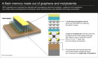
Like a sandwich
The transistor prototype developed by LANES was designed using "field effect" geometry, a bit like a sandwich. In the middle, instead of silicon, a thin layer of MoS2 channels electrons. Underneath, the electrodes transmitting electricity to the MoS2 layer are made out of graphene. And on top, the scientists also included an element made up of several layers of graphene; this captures electric charge and thus stores memory.
"Combining these two materials enabled us to make great progress in miniaturization, and also using these transistors we can make flexible nanoelectronic devices," explains Kis. The prototype stores a bit of memory, just a like a traditional cell. But according to the scientist, because molybdenite is thinner than silicon and thus more sensitive to charge, it offers great potential for more efficient data storage.
####
For more information, please click here
Contacts:
Andras Kis
41-216-933-925
Copyright © Ecole Polytechnique F�d�rale de Lausanne
If you have a comment, please Contact us.Issuers of news releases, not 7th Wave, Inc. or Nanotechnology Now, are solely responsible for the accuracy of the content.
Bookmark:


| Related News Press |
News and information
![]() Simulating magnetization in a Heisenberg quantum spin chain April 5th, 2024
Simulating magnetization in a Heisenberg quantum spin chain April 5th, 2024
![]() NRL charters Navy�s quantum inertial navigation path to reduce drift April 5th, 2024
NRL charters Navy�s quantum inertial navigation path to reduce drift April 5th, 2024
![]() Discovery points path to flash-like memory for storing qubits: Rice find could hasten development of nonvolatile quantum memory April 5th, 2024
Discovery points path to flash-like memory for storing qubits: Rice find could hasten development of nonvolatile quantum memory April 5th, 2024
Graphene/ Graphite
![]() NRL discovers two-dimensional waveguides February 16th, 2024
NRL discovers two-dimensional waveguides February 16th, 2024
Chip Technology
![]() Discovery points path to flash-like memory for storing qubits: Rice find could hasten development of nonvolatile quantum memory April 5th, 2024
Discovery points path to flash-like memory for storing qubits: Rice find could hasten development of nonvolatile quantum memory April 5th, 2024
![]() Utilizing palladium for addressing contact issues of buried oxide thin film transistors April 5th, 2024
Utilizing palladium for addressing contact issues of buried oxide thin film transistors April 5th, 2024
![]() HKUST researchers develop new integration technique for efficient coupling of III-V and silicon February 16th, 2024
HKUST researchers develop new integration technique for efficient coupling of III-V and silicon February 16th, 2024
Memory Technology
![]() Utilizing palladium for addressing contact issues of buried oxide thin film transistors April 5th, 2024
Utilizing palladium for addressing contact issues of buried oxide thin film transistors April 5th, 2024
![]() Interdisciplinary: Rice team tackles the future of semiconductors Multiferroics could be the key to ultralow-energy computing October 6th, 2023
Interdisciplinary: Rice team tackles the future of semiconductors Multiferroics could be the key to ultralow-energy computing October 6th, 2023
![]() Researchers discover materials exhibiting huge magnetoresistance June 9th, 2023
Researchers discover materials exhibiting huge magnetoresistance June 9th, 2023
Discoveries
![]() Chemical reactions can scramble quantum information as well as black holes April 5th, 2024
Chemical reactions can scramble quantum information as well as black holes April 5th, 2024
![]() New micromaterial releases nanoparticles that selectively destroy cancer cells April 5th, 2024
New micromaterial releases nanoparticles that selectively destroy cancer cells April 5th, 2024
![]() Utilizing palladium for addressing contact issues of buried oxide thin film transistors April 5th, 2024
Utilizing palladium for addressing contact issues of buried oxide thin film transistors April 5th, 2024
Announcements
![]() NRL charters Navy�s quantum inertial navigation path to reduce drift April 5th, 2024
NRL charters Navy�s quantum inertial navigation path to reduce drift April 5th, 2024
![]() Discovery points path to flash-like memory for storing qubits: Rice find could hasten development of nonvolatile quantum memory April 5th, 2024
Discovery points path to flash-like memory for storing qubits: Rice find could hasten development of nonvolatile quantum memory April 5th, 2024
|
|
||
|
|
||
| The latest news from around the world, FREE | ||
|
|
||
|
|
||
| Premium Products | ||
|
|
||
|
Only the news you want to read!
Learn More |
||
|
|
||
|
Full-service, expert consulting
Learn More |
||
|
|
||