Home > Press > Long Predicted Atomic Collapse State Observed in Graphene: Berkeley Lab researchers recreate elusive phenomenon with artificial nuclei
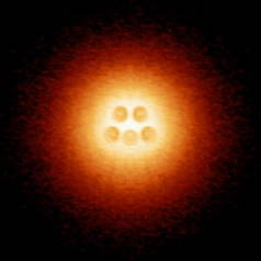 |
| An artificial atomic nucleus made up of five charged calcium dimers is centered in an atomic-collapse electron cloud. (Image courtesy of Michael Crommie) |
Abstract:
The first experimental observation of a quantum mechanical phenomenon that was predicted nearly 70 years ago holds important implications for the future of graphene-based electronic devices. Working with microscopic artificial atomic nuclei fabricated on graphene, a collaboration of researchers led by scientists with the U.S. Department of Energy's Lawrence Berkeley National Laboratory (Berkeley Lab) and the University of California (UC) Berkeley have imaged the "atomic collapse" states theorized to occur around super-large atomic nuclei.
Long Predicted Atomic Collapse State Observed in Graphene: Berkeley Lab researchers recreate elusive phenomenon with artificial nuclei
Berkeley, CA | Posted on March 13th, 2013"Atomic collapse is one of the holy grails of graphene research, as well as a holy grail of atomic and nuclear physics," says Michael Crommie, a physicist who holds joint appointments with Berkeley Lab's Materials Sciences Division and UC Berkeley's Physics Department. "While this work represents a very nice confirmation of basic relativistic quantum mechanics predictions made many decades ago, it is also highly relevant for future nanoscale devices where electrical charge is concentrated into very small areas."
Crommie is the corresponding author of a paper describing this work in the journal Science. The paper is titled "Observing Atomic Collapse Resonances in Artificial Nuclei on Graphene." Co-authors are Yang Wang, Dillon Wong, Andrey Shytov, Victor Brar, Sangkook Choi, Qiong Wu, Hsin-Zon Tsai, William Regan, Alex Zettl, Roland Kawakami, Steven Louie, and Leonid Levitov.
Originating from the ideas of quantum mechanics pioneer Paul Dirac, atomic collapse theory holds that when the positive electrical charge of a super-heavy atomic nucleus surpasses a critical threshold, the resulting strong Coulomb field causes a negatively charged electron to populate a state where the electron spirals down to the nucleus and then spirals away again, emitting a positron (a positively-charged electron) in the process. This highly unusual electronic state is a significant departure from what happens in a typical atom, where electrons occupy stable circular orbits around the nucleus.
"Nuclear physicists have tried to observe atomic collapse for many decades, but they never unambiguously saw the effect because it is so hard to make and maintain the necessary super-large nuclei," Crommie says. "Graphene has given us the opportunity to see a condensed matter analog of this behavior, since the extraordinary relativistic nature of electrons in graphene yields a much smaller nuclear charge threshold for creating the special supercritical nuclei that will exhibit atomic collapse behavior."
Perhaps no other material is currently generating as much excitement for new electronic technologies as graphene, sheets of pure carbon just one atom thick through which electrons can freely race 100 times faster than they move through silicon. Electrons moving through graphene's two-dimensional layer of carbon atoms, which are arranged in a hexagonally patterned honeycomb lattice, perfectly mimic the behavior of highly relativistic charged particles with no mass. Superthin, superstrong, superflexible, and superfast as an electrical conductor, graphene has been touted as a potential wonder material for a host of electronic applications, starting with ultrafast transistors.
In recent years scientists predicted that highly-charged impurities in graphene should exhibit a unique electronic resonance - a build-up of electrons partially localized in space and energy - corresponding to the atomic collapse state of super-large atomic nuclei. Last summer Crommie's team set the stage for experimentally verifying this prediction by confirming that graphene's electrons in the vicinity of charged atoms follow the rules of relativistic quantum mechanics. However, the charge on the atoms in that study was not yet large enough to see the elusive atomic collapse.
"Those results, however, were encouraging and indicated that we should be able to see the same atomic physics with highly charged impurities in graphene as the atomic collapse physics predicted for isolated atoms with highly charged nuclei," Crommie says. "That is to say, we should see an electron exhibiting a semiclassical inward spiral trajectory and a novel quantum mechanical state that is partially electron-like near the nucleus and partially hole-like far from the nucleus. For graphene we talk about �holes' instead of the positrons discussed by nuclear physicists."
To test this idea, Crommie and his research group used a specially equipped scanning tunneling microscope (STM) in ultra-high vacuum to construct, via atomic manipulation, artificial nuclei on the surface of a gated graphene device. The "nuclei" were actually clusters made up of pairs, or dimers, of calcium ions. With the STM, the researchers pushed calcium dimers together into a cluster, one by one, until the total charge in the cluster became supercritical. STM spectroscopy was then used to measure the spatial and energetic characteristics of the resulting atomic collapse electronic state around the supercritical impurity.
"The positively charged calcium dimers at the surface of graphene in our artificial nuclei played the same role that protons play in regular atomic nuclei," Crommie says. "By squeezing enough positive charge into a sufficiently small area, we were able to directly image how electrons behave around a nucleus as the nuclear charge is methodically increased from below the supercritical charge limit, where there is no atomic collapse, to above the supercritical charge limit, where atomic collapse occurs."
Observing atomic collapse physics in a condensed matter system is very different from observing it in a particle collider, Crommie says. Whereas in a particle collider the "smoking gun" evidence of atomic collapse is the emission of a positron from the supercritical nucleus, in a condensed matter system the smoking gun is the onset of a signature electronic state in the region nearby the supercritical nucleus. Crommie and his group observed this signature electronic state with artificial nuclei of three or more calcium dimers.
"The way in which we observe the atomic collapse state in condensed matter and think about it is quite different from how the nuclear and high-energy physicists think about it and how they have tried to observe it, but the heart of the physics is essentially the same," says Crommie.
If the immense promise of graphene-based electronic devices is to be fully realized, scientists and engineers will need to achieve a better understanding of phenomena such as this that involve the interactions of electrons with each other and with impurities in the material.
"Just as donor and acceptor states play a crucial role in understanding the behavior of conventional semiconductors, so too should atomic collapse states play a similar role in understanding the properties of defects and dopants in future graphene devices," Crommie says. "Because atomic collapse states are the most highly localized electronic states possible in pristine graphene, they also present completely new opportunities for directly exploring and understanding electronic behavior in graphene."
In addition to Berkeley Lab and UC Berkeley, other institutions represented in this work include UC Riverside, MIT, and the University of Exeter.
Berkeley Lab's work was supported by DOE's Office of Science. Other members of the research team received support from the Office of Naval Research and the National Science Foundation. Computational resources were provided by DOE at Berkeley Lab's NERSC facility.
####
About Berkeley Lab
Lawrence Berkeley National Laboratory (Berkeley Lab) addresses the world�s most urgent scientific challenges by advancing sustainable energy, protecting human health, creating new materials, and revealing the origin and fate of the universe. Founded in 1931, Berkeley Lab�s scientific expertise has been recognized with 13 Nobel prizes. The University of California manages Berkeley Lab for the U.S. Department of Energy�s Office of Science. For more, visit www.lbl.gov.
DOE�s Office of Science is the single largest supporter of basic research in the physical sciences in the United States, and is working to address some of the most pressing challenges of our time. For more information, please visit the Office of Science website at science.energy.gov.
For more information, please click here
Contacts:
Lynn Yarris
(510) 486-5375
Copyright © Berkeley
If you have a comment, please Contact us.Issuers of news releases, not 7th Wave, Inc. or Nanotechnology Now, are solely responsible for the accuracy of the content.
Bookmark:


| Related Links |
![]() For more about the research of Michael Crommie, go here:
For more about the research of Michael Crommie, go here:
| Related News Press |
Physics
![]() Simulating magnetization in a Heisenberg quantum spin chain April 5th, 2024
Simulating magnetization in a Heisenberg quantum spin chain April 5th, 2024
![]() Nanoscale CL thermometry with lanthanide-doped heavy-metal oxide in TEM March 8th, 2024
Nanoscale CL thermometry with lanthanide-doped heavy-metal oxide in TEM March 8th, 2024
![]() Optically trapped quantum droplets of light can bind together to form macroscopic complexes March 8th, 2024
Optically trapped quantum droplets of light can bind together to form macroscopic complexes March 8th, 2024
News and information
![]() Simulating magnetization in a Heisenberg quantum spin chain April 5th, 2024
Simulating magnetization in a Heisenberg quantum spin chain April 5th, 2024
![]() NRL charters Navy�s quantum inertial navigation path to reduce drift April 5th, 2024
NRL charters Navy�s quantum inertial navigation path to reduce drift April 5th, 2024
![]() Discovery points path to flash-like memory for storing qubits: Rice find could hasten development of nonvolatile quantum memory April 5th, 2024
Discovery points path to flash-like memory for storing qubits: Rice find could hasten development of nonvolatile quantum memory April 5th, 2024
Imaging
![]() Nanoscale CL thermometry with lanthanide-doped heavy-metal oxide in TEM March 8th, 2024
Nanoscale CL thermometry with lanthanide-doped heavy-metal oxide in TEM March 8th, 2024
Graphene/ Graphite
![]() NRL discovers two-dimensional waveguides February 16th, 2024
NRL discovers two-dimensional waveguides February 16th, 2024
Laboratories
![]() A battery�s hopping ions remember where they�ve been: Seen in atomic detail, the seemingly smooth flow of ions through a battery�s electrolyte is surprisingly complicated February 16th, 2024
A battery�s hopping ions remember where they�ve been: Seen in atomic detail, the seemingly smooth flow of ions through a battery�s electrolyte is surprisingly complicated February 16th, 2024
![]() NRL discovers two-dimensional waveguides February 16th, 2024
NRL discovers two-dimensional waveguides February 16th, 2024
Govt.-Legislation/Regulation/Funding/Policy
![]() NRL charters Navy�s quantum inertial navigation path to reduce drift April 5th, 2024
NRL charters Navy�s quantum inertial navigation path to reduce drift April 5th, 2024
![]() Discovery points path to flash-like memory for storing qubits: Rice find could hasten development of nonvolatile quantum memory April 5th, 2024
Discovery points path to flash-like memory for storing qubits: Rice find could hasten development of nonvolatile quantum memory April 5th, 2024
![]() Chemical reactions can scramble quantum information as well as black holes April 5th, 2024
Chemical reactions can scramble quantum information as well as black holes April 5th, 2024
Chip Technology
![]() Discovery points path to flash-like memory for storing qubits: Rice find could hasten development of nonvolatile quantum memory April 5th, 2024
Discovery points path to flash-like memory for storing qubits: Rice find could hasten development of nonvolatile quantum memory April 5th, 2024
![]() Utilizing palladium for addressing contact issues of buried oxide thin film transistors April 5th, 2024
Utilizing palladium for addressing contact issues of buried oxide thin film transistors April 5th, 2024
![]() HKUST researchers develop new integration technique for efficient coupling of III-V and silicon February 16th, 2024
HKUST researchers develop new integration technique for efficient coupling of III-V and silicon February 16th, 2024
Discoveries
![]() Chemical reactions can scramble quantum information as well as black holes April 5th, 2024
Chemical reactions can scramble quantum information as well as black holes April 5th, 2024
![]() New micromaterial releases nanoparticles that selectively destroy cancer cells April 5th, 2024
New micromaterial releases nanoparticles that selectively destroy cancer cells April 5th, 2024
![]() Utilizing palladium for addressing contact issues of buried oxide thin film transistors April 5th, 2024
Utilizing palladium for addressing contact issues of buried oxide thin film transistors April 5th, 2024
Materials/Metamaterials/Magnetoresistance
![]() Nanoscale CL thermometry with lanthanide-doped heavy-metal oxide in TEM March 8th, 2024
Nanoscale CL thermometry with lanthanide-doped heavy-metal oxide in TEM March 8th, 2024
![]() Focused ion beam technology: A single tool for a wide range of applications January 12th, 2024
Focused ion beam technology: A single tool for a wide range of applications January 12th, 2024
Announcements
![]() NRL charters Navy�s quantum inertial navigation path to reduce drift April 5th, 2024
NRL charters Navy�s quantum inertial navigation path to reduce drift April 5th, 2024
![]() Discovery points path to flash-like memory for storing qubits: Rice find could hasten development of nonvolatile quantum memory April 5th, 2024
Discovery points path to flash-like memory for storing qubits: Rice find could hasten development of nonvolatile quantum memory April 5th, 2024
Tools
![]() Ferroelectrically modulate the Fermi level of graphene oxide to enhance SERS response November 3rd, 2023
Ferroelectrically modulate the Fermi level of graphene oxide to enhance SERS response November 3rd, 2023
![]() The USTC realizes In situ electron paramagnetic resonance spectroscopy using single nanodiamond sensors November 3rd, 2023
The USTC realizes In situ electron paramagnetic resonance spectroscopy using single nanodiamond sensors November 3rd, 2023
Military
![]() NRL charters Navy�s quantum inertial navigation path to reduce drift April 5th, 2024
NRL charters Navy�s quantum inertial navigation path to reduce drift April 5th, 2024
![]() What heat can tell us about battery chemistry: using the Peltier effect to study lithium-ion cells March 8th, 2024
What heat can tell us about battery chemistry: using the Peltier effect to study lithium-ion cells March 8th, 2024
![]() New chip opens door to AI computing at light speed February 16th, 2024
New chip opens door to AI computing at light speed February 16th, 2024
Energy
![]() Development of zinc oxide nanopagoda array photoelectrode: photoelectrochemical water-splitting hydrogen production January 12th, 2024
Development of zinc oxide nanopagoda array photoelectrode: photoelectrochemical water-splitting hydrogen production January 12th, 2024
![]() Shedding light on unique conduction mechanisms in a new type of perovskite oxide November 17th, 2023
Shedding light on unique conduction mechanisms in a new type of perovskite oxide November 17th, 2023
![]() Inverted perovskite solar cell breaks 25% efficiency record: Researchers improve cell efficiency using a combination of molecules to address different November 17th, 2023
Inverted perovskite solar cell breaks 25% efficiency record: Researchers improve cell efficiency using a combination of molecules to address different November 17th, 2023
![]() The efficient perovskite cells with a structured anti-reflective layer � another step towards commercialization on a wider scale October 6th, 2023
The efficient perovskite cells with a structured anti-reflective layer � another step towards commercialization on a wider scale October 6th, 2023
Research partnerships
![]() Discovery points path to flash-like memory for storing qubits: Rice find could hasten development of nonvolatile quantum memory April 5th, 2024
Discovery points path to flash-like memory for storing qubits: Rice find could hasten development of nonvolatile quantum memory April 5th, 2024
![]() Researchers� approach may protect quantum computers from attacks March 8th, 2024
Researchers� approach may protect quantum computers from attacks March 8th, 2024
![]() 'Sudden death' of quantum fluctuations defies current theories of superconductivity: Study challenges the conventional wisdom of superconducting quantum transitions January 12th, 2024
'Sudden death' of quantum fluctuations defies current theories of superconductivity: Study challenges the conventional wisdom of superconducting quantum transitions January 12th, 2024
Quantum nanoscience
![]() Simulating magnetization in a Heisenberg quantum spin chain April 5th, 2024
Simulating magnetization in a Heisenberg quantum spin chain April 5th, 2024
![]() Optically trapped quantum droplets of light can bind together to form macroscopic complexes March 8th, 2024
Optically trapped quantum droplets of light can bind together to form macroscopic complexes March 8th, 2024
![]() Bridging light and electrons January 12th, 2024
Bridging light and electrons January 12th, 2024
![]() 'Sudden death' of quantum fluctuations defies current theories of superconductivity: Study challenges the conventional wisdom of superconducting quantum transitions January 12th, 2024
'Sudden death' of quantum fluctuations defies current theories of superconductivity: Study challenges the conventional wisdom of superconducting quantum transitions January 12th, 2024
|
|
||
|
|
||
| The latest news from around the world, FREE | ||
|
|
||
|
|
||
| Premium Products | ||
|
|
||
|
Only the news you want to read!
Learn More |
||
|
|
||
|
Full-service, expert consulting
Learn More |
||
|
|
||