Home > Press > New technique could improve optical devices
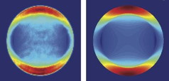 |
| The orientation of light emission The angular distribution of light emission from monolayer MoS2, left, closely matches the theoretical calculations for in-plane oriented emitters, right, indicating that light emission from MoS2 originates from in-plane oriented emitters. Credit: Zia lab/Brown University |
Abstract:
Understanding the source and orientation of light in light-emitting thin films — now possible with energy-momentum spectroscopy — could lead to better LEDs, solar cells, and other devices that use layered nanomaterials.
New technique could improve optical devices
Providence, RI | Posted on March 5th, 2013A multi-university research team has used a new spectroscopic method to gain a key insight into how light is emitted from layered nanomaterials and other thin films.
The technique, called energy-momentum spectroscopy, enables researchers to look at the light emerging from a thin film and determine whether it is coming from emitters oriented along the plane of the film or from emitters oriented perpendicular to the film. Knowing the orientations of emitters could help engineers make better use of thin-film materials in optical devices like LEDs or solar cells.
The research, published online on March 3 in Nature Nanotechnology, was a collaborative effort of Brown University, Case Western Reserve University, Columbia University, and the University of California-Santa Barbara.
The new technique takes advantage of a fundamental property of thin films: interference. Interference effects can be seen in the rainbow colors visible on the surface of soap bubbles or oil slicks. Scientists can analyze how light constructively and destructively interferes at different angles to draw conclusions about the film itself — how thick it is, for example. This new technique takes that kind of analysis one step further for light-emitting thin films.
"The key difference in our technique is we're looking at the energy as well as the angle and polarization at which light is emitted," said Rashid Zia, assistant professor of engineering at Brown University and one of the study's lead authors. "We can relate these different angles to distinct orientations of emitters in the film. At some angles and polarizations, we see only the light emission from in-plane emitters, while at other angles and polarizations we see only light originating from out-of-plane emitters."
The researchers demonstrated their technique on two important thin-film materials, molybdenum disulfide (MoS2) and PTCDA. Each represents a class of materials that shows promise for optical applications. MoS2 is a two-dimensional material similar to graphene, and PTCDA is an organic semiconductor. The research showed that light emission from MoS2 occurs only from in-plane emitters. In PTCDA, light comes from two distinct species of emitters, one in-plane and one out-of-plane.
####
About Brown University
Once the orientation of the emitters is known, Zia says, it may be possible to design structured devices that maximize those directional properties. In most applications, thin-film materials are layered on top of each other. The orientations of emitters in each layer indicate whether electronic excitations are happening within each layer or across layers, and that has implications for how such a device should be configured.
“If you were making an LED using these layered materials and you knew that the electronic excitations were happening across an interface,” Zia said, “then there’s a specific way you want to design the structure to get all of that light out and increase its overall efficiency.”
The same concept could apply to light-absorbing devices like solar cells. By understanding how the electronic excitations happen in the material, it could be possible to structure it in a way that coverts more incoming light to electricity.
“One of the exciting things about this research is how it brought together people with different expertise,” Zia said. “Our group’s expertise at Brown is in developing new forms of spectroscopy and studying the electronic origin of light emission. The Kymissis group at Columbia has a great deal of expertise in organic semiconductors, and the Shan group at Case Western has a great deal of expertise in layered nanomaterials. Jon Schuller, the study’s first author, did a great job in bringing all this expertise together. Jon was a visiting scientist here at Brown, a postdoctoral fellow in the Energy Frontier Research Center at Columbia, and is now a professor at UCSB.”
Other authors on the paper were Sinan Karaveli (Brown), Theanne Schiros (Columbia), Keliang He (Case Western), Shyuan Yang (Columbia), Ioannis Kymissis (Columbia) and Jie Shan (Case Western). Funding for the work was provided by the Air Force Office of Scientific Research, the Department of Energy, the National Science Foundation, and the Nanoelectronic Research Initiative of the Semiconductor Research Corporation.
For more information, please click here
Contacts:
Kevin Stacey
401-863-3766
Copyright © Brown University
If you have a comment, please Contact us.Issuers of news releases, not 7th Wave, Inc. or Nanotechnology Now, are solely responsible for the accuracy of the content.
Bookmark:


| Related News Press |
News and information
![]() Simulating magnetization in a Heisenberg quantum spin chain April 5th, 2024
Simulating magnetization in a Heisenberg quantum spin chain April 5th, 2024
![]() NRL charters Navy’s quantum inertial navigation path to reduce drift April 5th, 2024
NRL charters Navy’s quantum inertial navigation path to reduce drift April 5th, 2024
![]() Discovery points path to flash-like memory for storing qubits: Rice find could hasten development of nonvolatile quantum memory April 5th, 2024
Discovery points path to flash-like memory for storing qubits: Rice find could hasten development of nonvolatile quantum memory April 5th, 2024
![]() Good as gold - improving infectious disease testing with gold nanoparticles April 5th, 2024
Good as gold - improving infectious disease testing with gold nanoparticles April 5th, 2024
Thin films
![]() Utilizing palladium for addressing contact issues of buried oxide thin film transistors April 5th, 2024
Utilizing palladium for addressing contact issues of buried oxide thin film transistors April 5th, 2024
Display technology/LEDs/SS Lighting/OLEDs
![]() Utilizing palladium for addressing contact issues of buried oxide thin film transistors April 5th, 2024
Utilizing palladium for addressing contact issues of buried oxide thin film transistors April 5th, 2024
![]() Light guide plate based on perovskite nanocomposites November 3rd, 2023
Light guide plate based on perovskite nanocomposites November 3rd, 2023
![]() Simple ballpoint pen can write custom LEDs August 11th, 2023
Simple ballpoint pen can write custom LEDs August 11th, 2023
Govt.-Legislation/Regulation/Funding/Policy
![]() NRL charters Navy’s quantum inertial navigation path to reduce drift April 5th, 2024
NRL charters Navy’s quantum inertial navigation path to reduce drift April 5th, 2024
![]() Discovery points path to flash-like memory for storing qubits: Rice find could hasten development of nonvolatile quantum memory April 5th, 2024
Discovery points path to flash-like memory for storing qubits: Rice find could hasten development of nonvolatile quantum memory April 5th, 2024
![]() Chemical reactions can scramble quantum information as well as black holes April 5th, 2024
Chemical reactions can scramble quantum information as well as black holes April 5th, 2024
Discoveries
![]() Chemical reactions can scramble quantum information as well as black holes April 5th, 2024
Chemical reactions can scramble quantum information as well as black holes April 5th, 2024
![]() New micromaterial releases nanoparticles that selectively destroy cancer cells April 5th, 2024
New micromaterial releases nanoparticles that selectively destroy cancer cells April 5th, 2024
![]() Utilizing palladium for addressing contact issues of buried oxide thin film transistors April 5th, 2024
Utilizing palladium for addressing contact issues of buried oxide thin film transistors April 5th, 2024
Announcements
![]() NRL charters Navy’s quantum inertial navigation path to reduce drift April 5th, 2024
NRL charters Navy’s quantum inertial navigation path to reduce drift April 5th, 2024
![]() Discovery points path to flash-like memory for storing qubits: Rice find could hasten development of nonvolatile quantum memory April 5th, 2024
Discovery points path to flash-like memory for storing qubits: Rice find could hasten development of nonvolatile quantum memory April 5th, 2024
Tools
![]() Ferroelectrically modulate the Fermi level of graphene oxide to enhance SERS response November 3rd, 2023
Ferroelectrically modulate the Fermi level of graphene oxide to enhance SERS response November 3rd, 2023
![]() The USTC realizes In situ electron paramagnetic resonance spectroscopy using single nanodiamond sensors November 3rd, 2023
The USTC realizes In situ electron paramagnetic resonance spectroscopy using single nanodiamond sensors November 3rd, 2023
Military
![]() NRL charters Navy’s quantum inertial navigation path to reduce drift April 5th, 2024
NRL charters Navy’s quantum inertial navigation path to reduce drift April 5th, 2024
![]() What heat can tell us about battery chemistry: using the Peltier effect to study lithium-ion cells March 8th, 2024
What heat can tell us about battery chemistry: using the Peltier effect to study lithium-ion cells March 8th, 2024
![]() New chip opens door to AI computing at light speed February 16th, 2024
New chip opens door to AI computing at light speed February 16th, 2024
Energy
![]() Development of zinc oxide nanopagoda array photoelectrode: photoelectrochemical water-splitting hydrogen production January 12th, 2024
Development of zinc oxide nanopagoda array photoelectrode: photoelectrochemical water-splitting hydrogen production January 12th, 2024
![]() Shedding light on unique conduction mechanisms in a new type of perovskite oxide November 17th, 2023
Shedding light on unique conduction mechanisms in a new type of perovskite oxide November 17th, 2023
![]() Inverted perovskite solar cell breaks 25% efficiency record: Researchers improve cell efficiency using a combination of molecules to address different November 17th, 2023
Inverted perovskite solar cell breaks 25% efficiency record: Researchers improve cell efficiency using a combination of molecules to address different November 17th, 2023
![]() The efficient perovskite cells with a structured anti-reflective layer – another step towards commercialization on a wider scale October 6th, 2023
The efficient perovskite cells with a structured anti-reflective layer – another step towards commercialization on a wider scale October 6th, 2023
Grants/Sponsored Research/Awards/Scholarships/Gifts/Contests/Honors/Records
![]() Discovery points path to flash-like memory for storing qubits: Rice find could hasten development of nonvolatile quantum memory April 5th, 2024
Discovery points path to flash-like memory for storing qubits: Rice find could hasten development of nonvolatile quantum memory April 5th, 2024
![]() Chemical reactions can scramble quantum information as well as black holes April 5th, 2024
Chemical reactions can scramble quantum information as well as black holes April 5th, 2024
Research partnerships
![]() Discovery points path to flash-like memory for storing qubits: Rice find could hasten development of nonvolatile quantum memory April 5th, 2024
Discovery points path to flash-like memory for storing qubits: Rice find could hasten development of nonvolatile quantum memory April 5th, 2024
![]() Researchers’ approach may protect quantum computers from attacks March 8th, 2024
Researchers’ approach may protect quantum computers from attacks March 8th, 2024
![]() 'Sudden death' of quantum fluctuations defies current theories of superconductivity: Study challenges the conventional wisdom of superconducting quantum transitions January 12th, 2024
'Sudden death' of quantum fluctuations defies current theories of superconductivity: Study challenges the conventional wisdom of superconducting quantum transitions January 12th, 2024
Solar/Photovoltaic
![]() Development of zinc oxide nanopagoda array photoelectrode: photoelectrochemical water-splitting hydrogen production January 12th, 2024
Development of zinc oxide nanopagoda array photoelectrode: photoelectrochemical water-splitting hydrogen production January 12th, 2024
![]() Shedding light on unique conduction mechanisms in a new type of perovskite oxide November 17th, 2023
Shedding light on unique conduction mechanisms in a new type of perovskite oxide November 17th, 2023
![]() Inverted perovskite solar cell breaks 25% efficiency record: Researchers improve cell efficiency using a combination of molecules to address different November 17th, 2023
Inverted perovskite solar cell breaks 25% efficiency record: Researchers improve cell efficiency using a combination of molecules to address different November 17th, 2023
![]() Charged “molecular beasts” the basis for new compounds: Researchers at Leipzig University use “aggressive” fragments of molecular ions for chemical synthesis November 3rd, 2023
Charged “molecular beasts” the basis for new compounds: Researchers at Leipzig University use “aggressive” fragments of molecular ions for chemical synthesis November 3rd, 2023
|
|
||
|
|
||
| The latest news from around the world, FREE | ||
|
|
||
|
|
||
| Premium Products | ||
|
|
||
|
Only the news you want to read!
Learn More |
||
|
|
||
|
Full-service, expert consulting
Learn More |
||
|
|
||