Home > Press > Organic electronics -- how to make contact between carbon compounds and metal
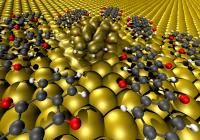 |
| Upon contact between the oxygen atoms protruding from the backbone and the metal, the molecules' internal structure changed in such a way that they lost their semiconducting properties and instead adopted the metallic properties of the surface.
Credit: Visualisation: Georg Heimel/HU Berlin |
Abstract:
Until now, however, it was practically impossible to accurately predict which molecules performed well on the job. They basically had to be identified by trial-and-error.
Now, an international team of scientists around Dr. Georg Heimel and Prof. Norbert Koch from the HZB and the Humboldt University Berlin has unraveled the mystery of what these molecules have in common. Their discovery enables more focused improvements to contact layers between metal electrodes and active materials in organic electronic devices.
Organic electronics -- how to make contact between carbon compounds and metal
Berlin, Germany | Posted on February 18th, 2013"We have been working on this question for a number of years now and could at last come up with a conclusive picture using a combination of several experimental methods and theoretical calculations," Georg Heimel explains. The researchers systematically examined different types of molecules whose backbones consist of the same chain of fused aromatic carbon rings. They differed in just one little detail: the number of oxygen atoms projecting from the backbone. These modified molecules were placed on the typical contact metals gold, silver, and copper.
Using photoelectron spectroscopy (UPS and XPS) at HZB's own BESSY II synchrotron radiation source, the researchers were able to identify chemical bonds that formed between the metal surfaces and the molecules as well as to measure the energy levels of the conduction electrons. Colleagues from Germany's T�bingen University determined the exact distance between the molecules and the metal surfaces using x-ray standing wave measurements taken at the ESRF synchrotron radiation source in Grenoble, France.
These experiments showed that, upon contact between the oxygen atoms protruding from the backbone and several of the metals, the molecules' internal structure changed in such a way that they lost their semiconducting properties and instead adopted the metallic properties of the surface. Despite similar prerequisites, this effect was not observed for the "bare"-backbone molecule. From the observation which molecules underwent these kinds of drastic changes on what metal, the researchers could derive general guidelines. "At this point, we have a pretty good sense of how molecules ought to look like and what their properties should be if they are to be good mediators between active organic materials and metal contacts, or, as we like to call it, good at forming soft metallic contacts," says Heimel.
Experts from a number of other German universities and from research facilities in Suzhou (China), Iwate and Chiba (Japan), and ESRF (France) have also contributed substantially to this publication.
####
For more information, please click here
Contacts:
Dr. Georg Heimel
Prof. Dr. Norbert Koch
Fon: +49 30-20 93 78 19
Copyright © Helmholtz Association of German Research Centres
If you have a comment, please Contact us.Issuers of news releases, not 7th Wave, Inc. or Nanotechnology Now, are solely responsible for the accuracy of the content.
Bookmark:


| Related News Press |
News and information
![]() Simulating magnetization in a Heisenberg quantum spin chain April 5th, 2024
Simulating magnetization in a Heisenberg quantum spin chain April 5th, 2024
![]() NRL charters Navy�s quantum inertial navigation path to reduce drift April 5th, 2024
NRL charters Navy�s quantum inertial navigation path to reduce drift April 5th, 2024
![]() Discovery points path to flash-like memory for storing qubits: Rice find could hasten development of nonvolatile quantum memory April 5th, 2024
Discovery points path to flash-like memory for storing qubits: Rice find could hasten development of nonvolatile quantum memory April 5th, 2024
![]() Good as gold - improving infectious disease testing with gold nanoparticles April 5th, 2024
Good as gold - improving infectious disease testing with gold nanoparticles April 5th, 2024
Display technology/LEDs/SS Lighting/OLEDs
![]() Utilizing palladium for addressing contact issues of buried oxide thin film transistors April 5th, 2024
Utilizing palladium for addressing contact issues of buried oxide thin film transistors April 5th, 2024
![]() Light guide plate based on perovskite nanocomposites November 3rd, 2023
Light guide plate based on perovskite nanocomposites November 3rd, 2023
![]() Simple ballpoint pen can write custom LEDs August 11th, 2023
Simple ballpoint pen can write custom LEDs August 11th, 2023
Chip Technology
![]() Discovery points path to flash-like memory for storing qubits: Rice find could hasten development of nonvolatile quantum memory April 5th, 2024
Discovery points path to flash-like memory for storing qubits: Rice find could hasten development of nonvolatile quantum memory April 5th, 2024
![]() Utilizing palladium for addressing contact issues of buried oxide thin film transistors April 5th, 2024
Utilizing palladium for addressing contact issues of buried oxide thin film transistors April 5th, 2024
![]() HKUST researchers develop new integration technique for efficient coupling of III-V and silicon February 16th, 2024
HKUST researchers develop new integration technique for efficient coupling of III-V and silicon February 16th, 2024
Discoveries
![]() Chemical reactions can scramble quantum information as well as black holes April 5th, 2024
Chemical reactions can scramble quantum information as well as black holes April 5th, 2024
![]() New micromaterial releases nanoparticles that selectively destroy cancer cells April 5th, 2024
New micromaterial releases nanoparticles that selectively destroy cancer cells April 5th, 2024
![]() Utilizing palladium for addressing contact issues of buried oxide thin film transistors April 5th, 2024
Utilizing palladium for addressing contact issues of buried oxide thin film transistors April 5th, 2024
Announcements
![]() NRL charters Navy�s quantum inertial navigation path to reduce drift April 5th, 2024
NRL charters Navy�s quantum inertial navigation path to reduce drift April 5th, 2024
![]() Discovery points path to flash-like memory for storing qubits: Rice find could hasten development of nonvolatile quantum memory April 5th, 2024
Discovery points path to flash-like memory for storing qubits: Rice find could hasten development of nonvolatile quantum memory April 5th, 2024
|
|
||
|
|
||
| The latest news from around the world, FREE | ||
|
|
||
|
|
||
| Premium Products | ||
|
|
||
|
Only the news you want to read!
Learn More |
||
|
|
||
|
Full-service, expert consulting
Learn More |
||
|
|
||