Home > Press > The world's most sensitive plasmon resonance sensor inspired by ancient Roman cup: World's most sensitive plasmon resonance sensor
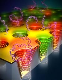 |
| This image shows a model of nano cup arrays.
Credit: University of Illinois at Urbana-Champaign |
Abstract:
Utilizing optical characteristics first demonstrated by the ancient Romans, researchers at the University of Illinois at Urbana-Champaign have created a novel, ultra-sensitive tool for chemical, DNA, and protein analysis.
The world's most sensitive plasmon resonance sensor inspired by ancient Roman cup: World's most sensitive plasmon resonance sensor
Urbana, IL | Posted on February 14th, 2013"With this device, the nanoplasmonic spectroscopy sensing, for the first time, becomes colorimetric sensing, requiring only naked eyes or ordinary visible color photography," explained Logan Liu, an assistant professor of electrical and computer engineering and of bioengineering at Illinois. "It can be used for chemical imaging, biomolecular imaging, and integration to portable microfluidics devices for lab-on-chip-applications. His research team's results were featured in the cover article of the inaugural edition of Advanced Optical Materials (AOM, optical section of Advanced Materials).
The Lycurgus cup was created by the Romans in 400 A.D. Made of a dichroic glass, the famous cup exhibits different colors depending on whether or not light is passing through it; red when lit from behind and green when lit from in front. It is also the origin of inspiration for all contemporary nanoplasmonics research�the study of optical phenomena in the nanoscale vicinity of metal surfaces.
"This dichroic effect was achieved by including tiny proportions of minutely ground gold and silver dust in the glass," Liu added. "In our research, we have created a large-area high density array of a nanoscale Lycurgus cup using a transparent plastic substrate to achieve colorimetric sensing. The sensor consists of about one billion nano cups in an array with sub-wavelength opening and decorated with metal nanoparticles on side walls, having similar shape and properties as the Lycurgus cups displayed in a British museum. Liu and his team were particularly excited by the extraordinary characteristics of the material, yielding 100 times better sensitivity than any other reported nanoplasmonic device.
Colorimetric techniques are mainly attractive because of their low cost, use of inexpensive equipment, requirement of fewer signal transduction hardware, and above all, providing simple-to-understand results. Colorimetric sensor can be used for both qualitative analytic identification as well as quantitative analysis. The current design will also enable new technology development in the field of DNA/protein microarray.
"Our label-free colorimetric sensor eliminates the need of problematic fluorescence tagging of DNA/ protein molecules, and the hybridization of probe and target molecule is detected from the color change of the sensor," stated Manas Gartia, first author of the article, "Colorimetrics: Colorimetric Plasmon Resonance Imaging Using Nano Lycurgus Cup Arrays." "Our current sensor requires just a light source and a camera to complete the DNA sensing process. This opens the possibility for developing affordable, simple and sensitive mobile phone-based DNA microarray detector in near future. Due to its low cost, simplicity in design, and high sensitivity, we envisage the extensive use of the device for DNA microarrays, therapeutic antibody screening for drug discovery, and pathogen detection in resource poor setting."
Gartia explained that light-matter interaction using sub-wavelength hole arrays gives rise to interesting optical phenomena such as surface plasmon polaritons (SPPs) mediated enhanced optical transmission (EOT). In case of EOT, more than expected amount of light can be transmitted through nanoholes on otherwise opaque metal thin films. Since the thin metal film has special optical property called surface plasmon resonance (SPR) which is affected by tiny amount surrounding materials, such device has been used as biosensing applications.
According to the researchers, most of the previous studies have mainly focused on manipulating in-plane two-dimensional (2D) EOT structures such as tuning the hole diameter, shape, or distance between the holes. In addition, most of the previous studies are concerned with straight holes only. Here, the EOT is mediated mainly by SPPs, which limits the sensitivity and figure of merits obtainable from such devices.
"Our current design employs 3D sub-wavelength tapered periodic hole array plasmonic structure. In contrast to the SPP mediated EOT, the proposed structure relies on Localized Surface Plasmon (LSP) mediated EOT," Gartia said. "The advantage of LSPs is that the enhanced transmission at different wavelengths and with different dispersion properties can be tuned by controlling the size, shape, and materials of the 3D holes. The tapered geometry will funnel and adiabatically focus the photons on to the sub-wavelength plasmonic structure at the bottom, leading to large local electric field and enhancement of EOT.
"Secondly the localized resonance supported by 3D plasmonic structure will enable broadband tuning of optical transmission through controlling the shape, size, and period of holes as well as the shape, size, and period of metallic particles decorated at the side walls. In other words, we will have more controllability over tuning the resonance wavelengths of the sensor."
In addition to Gartia and Liu, the paper's co-authors included Austin Hsiao, Anusha Pokhriyal, Sujin Seo, Gulsim Kulsharova, and Brian T. Cunningham at Illinois, and Tiziana C. Bond, at the Meso, Micro and Nano Technologies Center at Lawrence Livermore National Laboratory, California.
####
For more information, please click here
Contacts:
Logan Liu
217-244-4349
Copyright © University of Illinois College of Engineering
If you have a comment, please Contact us.Issuers of news releases, not 7th Wave, Inc. or Nanotechnology Now, are solely responsible for the accuracy of the content.
Bookmark:


| Related News Press |
Imaging
![]() Nanoscale CL thermometry with lanthanide-doped heavy-metal oxide in TEM March 8th, 2024
Nanoscale CL thermometry with lanthanide-doped heavy-metal oxide in TEM March 8th, 2024
Laboratories
![]() A battery�s hopping ions remember where they�ve been: Seen in atomic detail, the seemingly smooth flow of ions through a battery�s electrolyte is surprisingly complicated February 16th, 2024
A battery�s hopping ions remember where they�ve been: Seen in atomic detail, the seemingly smooth flow of ions through a battery�s electrolyte is surprisingly complicated February 16th, 2024
![]() NRL discovers two-dimensional waveguides February 16th, 2024
NRL discovers two-dimensional waveguides February 16th, 2024
Microfluidics/Nanofluidics
![]() Implantable device shrinks pancreatic tumors: Taming pancreatic cancer with intratumoral immunotherapy April 14th, 2023
Implantable device shrinks pancreatic tumors: Taming pancreatic cancer with intratumoral immunotherapy April 14th, 2023
![]() Researchers design new inks for 3D-printable wearable bioelectronics: Potential uses include printing electronic tattoos for medical tracking applications August 19th, 2022
Researchers design new inks for 3D-printable wearable bioelectronics: Potential uses include printing electronic tattoos for medical tracking applications August 19th, 2022
![]() Oregon State University research pushes closer to new therapy for pancreatic cancer May 6th, 2022
Oregon State University research pushes closer to new therapy for pancreatic cancer May 6th, 2022
Govt.-Legislation/Regulation/Funding/Policy
![]() NRL charters Navy�s quantum inertial navigation path to reduce drift April 5th, 2024
NRL charters Navy�s quantum inertial navigation path to reduce drift April 5th, 2024
![]() Discovery points path to flash-like memory for storing qubits: Rice find could hasten development of nonvolatile quantum memory April 5th, 2024
Discovery points path to flash-like memory for storing qubits: Rice find could hasten development of nonvolatile quantum memory April 5th, 2024
![]() Chemical reactions can scramble quantum information as well as black holes April 5th, 2024
Chemical reactions can scramble quantum information as well as black holes April 5th, 2024
Sensors
Discoveries
![]() Chemical reactions can scramble quantum information as well as black holes April 5th, 2024
Chemical reactions can scramble quantum information as well as black holes April 5th, 2024
![]() New micromaterial releases nanoparticles that selectively destroy cancer cells April 5th, 2024
New micromaterial releases nanoparticles that selectively destroy cancer cells April 5th, 2024
![]() Utilizing palladium for addressing contact issues of buried oxide thin film transistors April 5th, 2024
Utilizing palladium for addressing contact issues of buried oxide thin film transistors April 5th, 2024
Announcements
![]() NRL charters Navy�s quantum inertial navigation path to reduce drift April 5th, 2024
NRL charters Navy�s quantum inertial navigation path to reduce drift April 5th, 2024
![]() Discovery points path to flash-like memory for storing qubits: Rice find could hasten development of nonvolatile quantum memory April 5th, 2024
Discovery points path to flash-like memory for storing qubits: Rice find could hasten development of nonvolatile quantum memory April 5th, 2024
Tools
![]() Ferroelectrically modulate the Fermi level of graphene oxide to enhance SERS response November 3rd, 2023
Ferroelectrically modulate the Fermi level of graphene oxide to enhance SERS response November 3rd, 2023
![]() The USTC realizes In situ electron paramagnetic resonance spectroscopy using single nanodiamond sensors November 3rd, 2023
The USTC realizes In situ electron paramagnetic resonance spectroscopy using single nanodiamond sensors November 3rd, 2023
Photonics/Optics/Lasers
![]() With VECSELs towards the quantum internet Fraunhofer: IAF achieves record output power with VECSEL for quantum frequency converters April 5th, 2024
With VECSELs towards the quantum internet Fraunhofer: IAF achieves record output power with VECSEL for quantum frequency converters April 5th, 2024
![]() Nanoscale CL thermometry with lanthanide-doped heavy-metal oxide in TEM March 8th, 2024
Nanoscale CL thermometry with lanthanide-doped heavy-metal oxide in TEM March 8th, 2024
![]() Optically trapped quantum droplets of light can bind together to form macroscopic complexes March 8th, 2024
Optically trapped quantum droplets of light can bind together to form macroscopic complexes March 8th, 2024
![]() HKUST researchers develop new integration technique for efficient coupling of III-V and silicon February 16th, 2024
HKUST researchers develop new integration technique for efficient coupling of III-V and silicon February 16th, 2024
|
|
||
|
|
||
| The latest news from around the world, FREE | ||
|
|
||
|
|
||
| Premium Products | ||
|
|
||
|
Only the news you want to read!
Learn More |
||
|
|
||
|
Full-service, expert consulting
Learn More |
||
|
|
||