Home > Press > The Spark Within: Light-Emitting Bioprobe Fits in a Single Cell
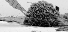 |
| This scanning electron microscope (SEM) image shows a nanobeam probe, including a large part of the handle tip, inserted in a typical cell. (Photo: Gary Shambat, Stanford School of Engineering) |
Abstract:
Stanford study is the first to demonstrate that sophisticated, engineered light resonators can be inserted inside cells without damaging the host. The researchers say it marks a new age in which tiny lasers and light-emitting diodes yield new avenues in the study and influence of living cells.
The Spark Within: Light-Emitting Bioprobe Fits in a Single Cell
Stanford, CA | Posted on February 13th, 2013If engineers at Stanford have their way, biological research may soon be transformed by a new class of light-emitting probes small enough to be injected into individual cells without harm to the host. Welcome to biophotonics, a discipline at the confluence of engineering, biology and medicine in which light-based devices - lasers and light-emitting diodes (LEDs) - are opening up new avenues in the study and influence of living cells.
The team described their probe in a paper published online February 13 by the journal Nano Letters. It is the first study to demonstrate that sophisticated engineered light resonators can be inserted inside cells without damaging the cell. Even with a resonator embedded inside, a cell is able to function, migrate and reproduce as normal.
Applications and implications
The researchers call their device a "nanobeam," because it resembles a steel I-beam with a series of round holes etched through the center. These beams, however, are not massive, but measure only a few microns in length and just a few hundred nanometers in width and thickness. It looks a bit like a piece from an erector set of old. The holes through the beams act like a nanoscale hall of mirrors, focusing and amplifying light at the center of the beam in what are known as photonic cavities. These are the building blocks for nanoscale lasers and LEDs.
"Devices like the photonic cavities we have built are quite possibly the most diverse and customizable ingredients in photonics," said the paper's senior author, Jelena Vuckovic, a professor of electrical engineering. "Applications span from fundamental physics to nanolasers and biosensors that could have profound impact on biological research."
At the cellular level, a nanobeam acts like a needle able to penetrate cell walls without injury. Once inserted, the beam emits light, yielding a remarkable array of research applications and implications. While other groups have shown that it is possible to insert simple nanotubes and electrical nanowires into cells, nobody had yet realized such complicated optical components inside biological cells.
"We think this is quite a dramatic shift from existing applications and will enable expanded opportunities for understanding and influencing cellular biology," said the paper's first author Gary Shambat, a doctoral candidate in electrical engineering. Shambat works at the Nanoscale and Quantum Photonics Lab directed by Vuckovic.
Iron to a magnet
In this case, the studied cells came from a prostate tumor, indicating possible application for the probe in cancer research. The primary and most immediate use would be in the real-time sensing of specific proteins within the cells, but the probe could be adapted to sense any important biomolecules such as DNA or RNA.
To detect these key molecules, researchers coat the probe with certain organic molecules or antibodies that are known to attract the target proteins, just like iron to a magnet. If the desired proteins are present within the cell, they begin to accumulate on the probe and cause a slight-but-detectable shift in the wavelength of the light being emitted from the device. This shift is a positive indication that the protein is present and in what quantity.
"Let's say you have a study that is interested in whether a certain drug produces or inhibits a specific protein. Our biosensor would tell definitively if the drug was working and how well based on the color of the light from the probe. It would be quite a powerful tool," explained Sanjiv Sam Gambhir, MD, co-author of the paper and chair of the Department of Radiology at the Stanford School of Medicine as well as director of Stanford's Canary Center for Early Cancer Detection.
As such, embeddable nanoscale optical sensors would represent a key development in the quest for patient-specific cancer therapies�often referred to as personalized medicine�in which drugs are targeted to the patient based on efficacy.
A clever structure
Structurally, the new device is a sandwich of extremely thin layers of the semiconductor gallium arsenide alternated with similarly thin layers of light-emitting crystal, a sort of photonic fuel known as quantum dots. The structure is carved out of chips or wafers, much like sculptures are chiseled out of rock. Once sculpted, the devices remain tethered to the thick substrate.
Shambat and his fellow engineers have been working on similar optical devices for use in ultrafast, ultra-efficient computer applications where having devices immobilized on chips and wafers does not matter so much since they will ultimately be integrated with microelectronics.
For biological applications, however, the thick, heavy substrate presents a serious hurdle for interfacing with single-cells. The underlying and all-important nanocavities are locked in position on the rigid material and unable to penetrate cell walls.
Shambat's breakthrough came when he was able to peel away the photonic nanobeams, leaving the bulky wafer behind. He then glued the ultrathin photonic device to a fiber optic cable with which he steers the needle-like probe toward and into the cell.
Similarly, anticipating that gallium arsenide could be toxic to cells, Shambat also devised a clever way to encapsulate his devices in a thin, electrically insulating coating of alumina and zirconia. The coating serves two purposes: it both protects the cell from the potentially toxic gallium arsenide and protects the probe from degrading in the cell environment.
"Stunning" results
Once inserted in the cell, the probe emits light, which can be observed from outside. For engineers, it means that almost any current application or use of these powerful photonic devices can be translated into the previously off-limits environment of the cell interior.
In one finding that the authors describe as stunning, they loaded their nanobeams into cells and watched as the cells grew, migrated around the research environment and reproduced. Each time a cell divided, one of the daughter cells inherited the nanobeam from the parent and the beam continued to function as expected.
This inheritability frees researchers to study living cells over long periods of time, a research advantage not possible with existing detection techniques, which require cells be either dead or fixed in place.
"Our nanoscale probes can reside in cells for long periods of time, potentially providing sensor feedback or giving control signals to the cells down the road," said Shambat. "We tracked one cell for eight days. That's a long time for a single-cell study."
Other contributing authors of the study include post-doctoral scholar Sri-Rajasekhar Kothapalli, research associate J Provine, doctoral candidate Tomas Sarmiento and Professor James Harris.
Funding for this study was provided by The Beckman Center for Molecular and Genetic Medicine at Stanford, the Canary Foundation and the Center for Cancer and Nanotechnology Excellence.
By Andrew Myers
Andrew Myers is associate director of communications for the Stanford University School of Engineering.
####
For more information, please click here
Contacts:
Andrew Myers
650-736-2245
Copyright © Stanford School of Engineering
If you have a comment, please Contact us.Issuers of news releases, not 7th Wave, Inc. or Nanotechnology Now, are solely responsible for the accuracy of the content.
Bookmark:


| Related News Press |
News and information
![]() Simulating magnetization in a Heisenberg quantum spin chain April 5th, 2024
Simulating magnetization in a Heisenberg quantum spin chain April 5th, 2024
![]() NRL charters Navy�s quantum inertial navigation path to reduce drift April 5th, 2024
NRL charters Navy�s quantum inertial navigation path to reduce drift April 5th, 2024
![]() Discovery points path to flash-like memory for storing qubits: Rice find could hasten development of nonvolatile quantum memory April 5th, 2024
Discovery points path to flash-like memory for storing qubits: Rice find could hasten development of nonvolatile quantum memory April 5th, 2024
![]() Good as gold - improving infectious disease testing with gold nanoparticles April 5th, 2024
Good as gold - improving infectious disease testing with gold nanoparticles April 5th, 2024
Display technology/LEDs/SS Lighting/OLEDs
![]() Utilizing palladium for addressing contact issues of buried oxide thin film transistors April 5th, 2024
Utilizing palladium for addressing contact issues of buried oxide thin film transistors April 5th, 2024
![]() Light guide plate based on perovskite nanocomposites November 3rd, 2023
Light guide plate based on perovskite nanocomposites November 3rd, 2023
![]() Simple ballpoint pen can write custom LEDs August 11th, 2023
Simple ballpoint pen can write custom LEDs August 11th, 2023
Nanomedicine
![]() New micromaterial releases nanoparticles that selectively destroy cancer cells April 5th, 2024
New micromaterial releases nanoparticles that selectively destroy cancer cells April 5th, 2024
![]() Good as gold - improving infectious disease testing with gold nanoparticles April 5th, 2024
Good as gold - improving infectious disease testing with gold nanoparticles April 5th, 2024
![]() Researchers develop artificial building blocks of life March 8th, 2024
Researchers develop artificial building blocks of life March 8th, 2024
Discoveries
![]() Chemical reactions can scramble quantum information as well as black holes April 5th, 2024
Chemical reactions can scramble quantum information as well as black holes April 5th, 2024
![]() New micromaterial releases nanoparticles that selectively destroy cancer cells April 5th, 2024
New micromaterial releases nanoparticles that selectively destroy cancer cells April 5th, 2024
![]() Utilizing palladium for addressing contact issues of buried oxide thin film transistors April 5th, 2024
Utilizing palladium for addressing contact issues of buried oxide thin film transistors April 5th, 2024
Announcements
![]() NRL charters Navy�s quantum inertial navigation path to reduce drift April 5th, 2024
NRL charters Navy�s quantum inertial navigation path to reduce drift April 5th, 2024
![]() Discovery points path to flash-like memory for storing qubits: Rice find could hasten development of nonvolatile quantum memory April 5th, 2024
Discovery points path to flash-like memory for storing qubits: Rice find could hasten development of nonvolatile quantum memory April 5th, 2024
Nanobiotechnology
![]() New micromaterial releases nanoparticles that selectively destroy cancer cells April 5th, 2024
New micromaterial releases nanoparticles that selectively destroy cancer cells April 5th, 2024
![]() Good as gold - improving infectious disease testing with gold nanoparticles April 5th, 2024
Good as gold - improving infectious disease testing with gold nanoparticles April 5th, 2024
![]() Researchers develop artificial building blocks of life March 8th, 2024
Researchers develop artificial building blocks of life March 8th, 2024
Photonics/Optics/Lasers
![]() With VECSELs towards the quantum internet Fraunhofer: IAF achieves record output power with VECSEL for quantum frequency converters April 5th, 2024
With VECSELs towards the quantum internet Fraunhofer: IAF achieves record output power with VECSEL for quantum frequency converters April 5th, 2024
![]() Nanoscale CL thermometry with lanthanide-doped heavy-metal oxide in TEM March 8th, 2024
Nanoscale CL thermometry with lanthanide-doped heavy-metal oxide in TEM March 8th, 2024
![]() Optically trapped quantum droplets of light can bind together to form macroscopic complexes March 8th, 2024
Optically trapped quantum droplets of light can bind together to form macroscopic complexes March 8th, 2024
![]() HKUST researchers develop new integration technique for efficient coupling of III-V and silicon February 16th, 2024
HKUST researchers develop new integration technique for efficient coupling of III-V and silicon February 16th, 2024
|
|
||
|
|
||
| The latest news from around the world, FREE | ||
|
|
||
|
|
||
| Premium Products | ||
|
|
||
|
Only the news you want to read!
Learn More |
||
|
|
||
|
Full-service, expert consulting
Learn More |
||
|
|
||