Home > Press > Using single quantum dots to probe nanowires: Lighting up plasmonic wires with nanometer accuracy
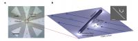 |
| (a) This is an optical image of the microfluidic crossed-channel device. Flow in the center control region (dashed circle) is manipulated in two dimensions by 4 external electrodes (not shown). Scale bar is 500 μm. (b) This is a schematic of the positioning and imaging technique. A single QD is driven along a trajectory close to the wire by flow control. The inset shows a microcope image of a typical nanowire with 1 μm scale bar.
Credit: JQI |
Abstract:
Modern telecommunications happens because of fast electrons and fast photons. Can it get better? Can Moore's law---the doubling of computing power ever 18 months or so---be sustained? Can the compactness (nm-scale components) of electronics be combined with the speed of photonics? Well, one such hybrid approach is being explored at the Joint Quantum Institute (*), where scientists bring together three marvelous physics research fields: microfluidics, quantum dots, and plasmonics to probe and study optical nanostructures with spatial accuracy as fine as 12 nm.
Using single quantum dots to probe nanowires: Lighting up plasmonic wires with nanometer accuracy
College Park, MD | Posted on February 5th, 2013PLASMONICS
When light strikes a strip of metal an electron wave can be excited in the surface. Is this "surface plasmon" a bit of light or electricity. Well, it's a bit of both. The wavelength of this electromagnetic wave is shorter and the energy density higher than that of the incoming laser light; the plasmon is thus tightly localized light constrained to propagate along the meal surface. The science of "plasmonics" has arisen to capitalize on various imaging, sensing, and processing abilities inherent in plasmons. To start with, though, one needs to know exactly what happens at that laser-excited metallic surface. That light is converted into the plasmonic wave; later the energy can be reconverted into light.
Here's where the JQI experiment comes in. The main result of the work, published February 5 in the journal Nature Communications, is to provide a map showing how the metal strip, in this case a silver wire 4 microns long and 100 nm wide, lights up.
MICROFLUIDICS AND QUANTUM DOTS
The other two chief components of the experiment, in addition to plasmonics, are microfluidics and quantum dots. Microfluidics, a relatively new science all by itself, features the movement of nanoliter volumes of fluids through channels defined on microchips, analogous to the conducting paths strung across microprocessors for carrying electrical currents. Quantum dots, nanometer-sized semiconductor balls, are tailored to possess a specified set of allowed energy states; in effect the dots are artificial atoms that can be moved around. In the JQI experiment the 10-nm-wide dots (the important cadmium-selenide layer is only 3 nm thick) float in a fluid whose flow can be controlled by varying an applied voltage. The dots are drawn up close to the nanowire as if they were mines next to a submarine.
Indeed the dot is there precisely to excite the wire. The dot is fluorescence machine---in a loose sense a nanoscopic lightbulb. Striking it with green laser light, it quickly re-emits red light (one photon at a time), and it is this radiation which excites waves in the nearby wire, which acts like an antenna. But the interaction is a two-way street; the dot's emissions will vary depending on where along the length of the wire it is; the end of the wire (like any pointy lightning rod on a barn) is where electrical fields are highest and this attracts the most emission from the dot.
A CCD camera captures light coming from the dots and from the wire. The camera qualities, the optical properties of the dot, the careful positioning of the dot, and the shape and purity of the nanowire combine to provide an image of the electric field intensity of the nanowire with 12-nm accuracy. The intensity map shows that the input red light from the quantum dot (wavelength of 620 nm) has effectively been transformed into a plasmonic wavelength of 320 nm.
Chad Ropp is a graduate student working on the project and the lead author on the paper. "Plasmonic maps have been resolved before, but the quantum mechanical interactions with a single emitter have not, and not with this degree of accuracy," said Ropp.
POSSIBLE APPLICATIONS
In an actual device, the quantum dot could be replaced by a bio-particle which could be identified through the nanowire's observed effect on particle's emissions. Or the dot-wire duo could be combined in various configurations as plasmonic equivalents of electronic circuit components. Other uses for this kind of nanowire setup might exploit the high energy density in the plasmonic state to support nonlinear effects. This could enable the nanowire-dot combination to operate as an optical transistor.
"Nanoscale imaging and spontaneous emission control with a single nano-positioned quantum dot," Chad Ropp, Zachary Cummins, Sanghee Nah, John T. Fourkas, Benjamin Shapiro, Edo Waks, Nature Communications, paper published online 5 February 2013. Chad Ropp, , 301-405-5010
####
About Joint Quantum Institute
The Joint Quantum Institute is operated jointly by the National Institute of Standards and Technology in Gaithersburg, MD and the University of Maryland in College Park.
For more information, please click here
Contacts:
Phillip F. Schewe
301-405-0989
Copyright © Joint Quantum Institute
If you have a comment, please Contact us.Issuers of news releases, not 7th Wave, Inc. or Nanotechnology Now, are solely responsible for the accuracy of the content.
Bookmark:


| Related News Press |
News and information
![]() Simulating magnetization in a Heisenberg quantum spin chain April 5th, 2024
Simulating magnetization in a Heisenberg quantum spin chain April 5th, 2024
![]() NRL charters Navy�s quantum inertial navigation path to reduce drift April 5th, 2024
NRL charters Navy�s quantum inertial navigation path to reduce drift April 5th, 2024
![]() Discovery points path to flash-like memory for storing qubits: Rice find could hasten development of nonvolatile quantum memory April 5th, 2024
Discovery points path to flash-like memory for storing qubits: Rice find could hasten development of nonvolatile quantum memory April 5th, 2024
Laboratories
![]() A battery�s hopping ions remember where they�ve been: Seen in atomic detail, the seemingly smooth flow of ions through a battery�s electrolyte is surprisingly complicated February 16th, 2024
A battery�s hopping ions remember where they�ve been: Seen in atomic detail, the seemingly smooth flow of ions through a battery�s electrolyte is surprisingly complicated February 16th, 2024
![]() NRL discovers two-dimensional waveguides February 16th, 2024
NRL discovers two-dimensional waveguides February 16th, 2024
![]() Three-pronged approach discerns qualities of quantum spin liquids November 17th, 2023
Three-pronged approach discerns qualities of quantum spin liquids November 17th, 2023
Microfluidics/Nanofluidics
![]() Implantable device shrinks pancreatic tumors: Taming pancreatic cancer with intratumoral immunotherapy April 14th, 2023
Implantable device shrinks pancreatic tumors: Taming pancreatic cancer with intratumoral immunotherapy April 14th, 2023
![]() Researchers design new inks for 3D-printable wearable bioelectronics: Potential uses include printing electronic tattoos for medical tracking applications August 19th, 2022
Researchers design new inks for 3D-printable wearable bioelectronics: Potential uses include printing electronic tattoos for medical tracking applications August 19th, 2022
![]() Oregon State University research pushes closer to new therapy for pancreatic cancer May 6th, 2022
Oregon State University research pushes closer to new therapy for pancreatic cancer May 6th, 2022
Govt.-Legislation/Regulation/Funding/Policy
![]() NRL charters Navy�s quantum inertial navigation path to reduce drift April 5th, 2024
NRL charters Navy�s quantum inertial navigation path to reduce drift April 5th, 2024
![]() Discovery points path to flash-like memory for storing qubits: Rice find could hasten development of nonvolatile quantum memory April 5th, 2024
Discovery points path to flash-like memory for storing qubits: Rice find could hasten development of nonvolatile quantum memory April 5th, 2024
![]() Chemical reactions can scramble quantum information as well as black holes April 5th, 2024
Chemical reactions can scramble quantum information as well as black holes April 5th, 2024
Chip Technology
![]() Discovery points path to flash-like memory for storing qubits: Rice find could hasten development of nonvolatile quantum memory April 5th, 2024
Discovery points path to flash-like memory for storing qubits: Rice find could hasten development of nonvolatile quantum memory April 5th, 2024
![]() Utilizing palladium for addressing contact issues of buried oxide thin film transistors April 5th, 2024
Utilizing palladium for addressing contact issues of buried oxide thin film transistors April 5th, 2024
![]() HKUST researchers develop new integration technique for efficient coupling of III-V and silicon February 16th, 2024
HKUST researchers develop new integration technique for efficient coupling of III-V and silicon February 16th, 2024
Optical computing/Photonic computing
![]() With VECSELs towards the quantum internet Fraunhofer: IAF achieves record output power with VECSEL for quantum frequency converters April 5th, 2024
With VECSELs towards the quantum internet Fraunhofer: IAF achieves record output power with VECSEL for quantum frequency converters April 5th, 2024
![]() Chemical reactions can scramble quantum information as well as black holes April 5th, 2024
Chemical reactions can scramble quantum information as well as black holes April 5th, 2024
![]() Optically trapped quantum droplets of light can bind together to form macroscopic complexes March 8th, 2024
Optically trapped quantum droplets of light can bind together to form macroscopic complexes March 8th, 2024
![]() HKUST researchers develop new integration technique for efficient coupling of III-V and silicon February 16th, 2024
HKUST researchers develop new integration technique for efficient coupling of III-V and silicon February 16th, 2024
Discoveries
![]() Chemical reactions can scramble quantum information as well as black holes April 5th, 2024
Chemical reactions can scramble quantum information as well as black holes April 5th, 2024
![]() New micromaterial releases nanoparticles that selectively destroy cancer cells April 5th, 2024
New micromaterial releases nanoparticles that selectively destroy cancer cells April 5th, 2024
![]() Utilizing palladium for addressing contact issues of buried oxide thin film transistors April 5th, 2024
Utilizing palladium for addressing contact issues of buried oxide thin film transistors April 5th, 2024
Announcements
![]() NRL charters Navy�s quantum inertial navigation path to reduce drift April 5th, 2024
NRL charters Navy�s quantum inertial navigation path to reduce drift April 5th, 2024
![]() Discovery points path to flash-like memory for storing qubits: Rice find could hasten development of nonvolatile quantum memory April 5th, 2024
Discovery points path to flash-like memory for storing qubits: Rice find could hasten development of nonvolatile quantum memory April 5th, 2024
Quantum Dots/Rods
![]() A new kind of magnetism November 17th, 2023
A new kind of magnetism November 17th, 2023
![]() IOP Publishing celebrates World Quantum Day with the announcement of a special quantum collection and the winners of two prestigious quantum awards April 14th, 2023
IOP Publishing celebrates World Quantum Day with the announcement of a special quantum collection and the winners of two prestigious quantum awards April 14th, 2023
![]() Qubits on strong stimulants: Researchers find ways to improve the storage time of quantum information in a spin rich material January 27th, 2023
Qubits on strong stimulants: Researchers find ways to improve the storage time of quantum information in a spin rich material January 27th, 2023
![]() NIST�s grid of quantum islands could reveal secrets for powerful technologies November 18th, 2022
NIST�s grid of quantum islands could reveal secrets for powerful technologies November 18th, 2022
Photonics/Optics/Lasers
![]() With VECSELs towards the quantum internet Fraunhofer: IAF achieves record output power with VECSEL for quantum frequency converters April 5th, 2024
With VECSELs towards the quantum internet Fraunhofer: IAF achieves record output power with VECSEL for quantum frequency converters April 5th, 2024
![]() Nanoscale CL thermometry with lanthanide-doped heavy-metal oxide in TEM March 8th, 2024
Nanoscale CL thermometry with lanthanide-doped heavy-metal oxide in TEM March 8th, 2024
![]() Optically trapped quantum droplets of light can bind together to form macroscopic complexes March 8th, 2024
Optically trapped quantum droplets of light can bind together to form macroscopic complexes March 8th, 2024
![]() HKUST researchers develop new integration technique for efficient coupling of III-V and silicon February 16th, 2024
HKUST researchers develop new integration technique for efficient coupling of III-V and silicon February 16th, 2024
Alliances/Trade associations/Partnerships/Distributorships
![]() Chicago Quantum Exchange welcomes six new partners highlighting quantum technology solutions, from Chicago and beyond September 23rd, 2022
Chicago Quantum Exchange welcomes six new partners highlighting quantum technology solutions, from Chicago and beyond September 23rd, 2022
![]() University of Illinois Chicago joins Brookhaven Lab's Quantum Center June 10th, 2022
University of Illinois Chicago joins Brookhaven Lab's Quantum Center June 10th, 2022
Research partnerships
![]() Discovery points path to flash-like memory for storing qubits: Rice find could hasten development of nonvolatile quantum memory April 5th, 2024
Discovery points path to flash-like memory for storing qubits: Rice find could hasten development of nonvolatile quantum memory April 5th, 2024
![]() Researchers� approach may protect quantum computers from attacks March 8th, 2024
Researchers� approach may protect quantum computers from attacks March 8th, 2024
![]() 'Sudden death' of quantum fluctuations defies current theories of superconductivity: Study challenges the conventional wisdom of superconducting quantum transitions January 12th, 2024
'Sudden death' of quantum fluctuations defies current theories of superconductivity: Study challenges the conventional wisdom of superconducting quantum transitions January 12th, 2024
|
|
||
|
|
||
| The latest news from around the world, FREE | ||
|
|
||
|
|
||
| Premium Products | ||
|
|
||
|
Only the news you want to read!
Learn More |
||
|
|
||
|
Full-service, expert consulting
Learn More |
||
|
|
||