Home > Press > Light-emitting triangles may have applications in optical technology
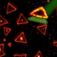 |
| Triangular single layers of tungsten disulfide have been synthesized by Penn State researchers. The edges of the triangles exhibit extraordinary photoluminescence, while the interior area does not. The photoluminescent signal disappears as the number of layers increases. These triangular structures may have potential applications in optical technology; for example, for use in light detectors and lasers.
Credit: Terrones lab, Penn State Universtiy |
Abstract:
For the first time, scientists have created single layers of a naturally occurring rare mineral called tungstenite, or WS2. The resulting sheet of stacked sulfur and tungsten atoms forms a honeycomb pattern of triangles that have been shown to have unusual light-emitting, or photoluminescent, properties. According to team leader Mauricio Terrones, a professor of physics and of materials science and engineering at Penn State, the triangular structures have potential applications in optical technology; for example, for use in light detectors and lasers. The results of the research will be published in a print edition of the journal NANO Letters.
Light-emitting triangles may have applications in optical technology
University Park, PA | Posted on February 5th, 2013Terrones explained that creating monolayers -- single, one-atom-thick layers -- is of special interest to scientists because the chemical properties of minerals and other substances are known to change depending on their atomic thickness, opening the door to potentially useful applications of multi-layered materials of various thicknesses. In previous research, scientists had accomplished the feat of making a monolayer of graphene -- a substance similar to the graphite found in pencil leads. "The technique these researchers used was tedious, but it worked," Terrones said. "They basically removed, or exfoliated, the graphene, layer by layer, with Scotch tape, until they got down to a single atom of thickness."
Now, for the first time, Terrones and his team have used a controlled thermal reduction-sulfurization method -- or chemical vapor deposition -- to accomplish the same feat with a rare mineral called tungstenite. The scientists began by depositing tiny crystals of tungsten oxide, which are less than one nanometer in height, and they then passed the crystals through sulfur vapor at 850 degrees Celsius. This process led to individual layers -- or sheets -- composed of one atom in thickness. The resulting structure -- called tungsten disulfide -- is a honeycomb pattern of triangles consisting of tungsten atoms bonded with sulfur atoms.
"One of the most exciting properties of the tungsten disulfide monolayer is its photoluminescence," Terrones said. Terrones explained that photoluminescence occurs when a substance absorbs light at one wavelength and re-emits that light at a different wavelength. The property of photoluminescence also occurs in certain bioluminescenent animals such as angler fish and fireflies. "One interesting discovery from our work is the fact that we see the strongest photoluminescence at the edges of the triangles, right where the chemistry of the atoms changes, with much less photoluminescence occurring in the center of the triangles," Terrones said. "We also have found that these new monolayers luminesce at room temperature. So no special temperature requirements are needed for the material to exhibit this property."
Co-author Vincent H. Crespi, Distinguished Professor of Physics, Chemistry, and Materials Science and Engineering at Penn State, added, "The images of the photoluminescence are beautiful; the triangles light up all around their edges like little holiday ornaments -- holiday ornaments with potentially transformative, long-term applications in nano-optics."
The research has many potential applications in the fields of optical light detection, the production of light-emitting diodes, and even laser technology. The researchers also plan to try the chemical-vapor-deposition technology to grow innovative monolayers using other layered materials with potentially useful applications.
In addition to Terrones and Crespi, other researchers who contributed to this study include Humberto R. Guti�rrez, an assistant professor at the University of Louisville; Nestor Perea-L�pez and Ana Laura El�as, research associates at Penn State; Ayse Berkdemir and Ruitao Lv, posdoctoral fellows at Penn State; Bei Wang and Yuanxi Wang, graduate students at Penn State; and Florentino L�pez-Ur�as and Humberto Terrones, visiting professors at Penn State.
Support for this research comes primarily from the U.S. Army Research Office and, in part, from the Penn State Center for Nanoscale Science.
[ Katrina Voss ]
GRANT NUMBERS: U.S. Army Research Office (MURI grant W911NF-11-1-0362), Penn State Center for Nanoscale Science (DMR-0820404)
####
For more information, please click here
Contacts:
Barbara Kennedy
814-863-4682
Mauricio Terrones:
814-865-0343
Vincent H. Crespi
814-863-0163
Copyright © Penn State
If you have a comment, please Contact us.Issuers of news releases, not 7th Wave, Inc. or Nanotechnology Now, are solely responsible for the accuracy of the content.
Bookmark:


| Related News Press |
News and information
![]() Simulating magnetization in a Heisenberg quantum spin chain April 5th, 2024
Simulating magnetization in a Heisenberg quantum spin chain April 5th, 2024
![]() NRL charters Navy�s quantum inertial navigation path to reduce drift April 5th, 2024
NRL charters Navy�s quantum inertial navigation path to reduce drift April 5th, 2024
![]() Discovery points path to flash-like memory for storing qubits: Rice find could hasten development of nonvolatile quantum memory April 5th, 2024
Discovery points path to flash-like memory for storing qubits: Rice find could hasten development of nonvolatile quantum memory April 5th, 2024
![]() Good as gold - improving infectious disease testing with gold nanoparticles April 5th, 2024
Good as gold - improving infectious disease testing with gold nanoparticles April 5th, 2024
Display technology/LEDs/SS Lighting/OLEDs
![]() Utilizing palladium for addressing contact issues of buried oxide thin film transistors April 5th, 2024
Utilizing palladium for addressing contact issues of buried oxide thin film transistors April 5th, 2024
Chemistry
![]() What heat can tell us about battery chemistry: using the Peltier effect to study lithium-ion cells March 8th, 2024
What heat can tell us about battery chemistry: using the Peltier effect to study lithium-ion cells March 8th, 2024
![]() Nanoscale CL thermometry with lanthanide-doped heavy-metal oxide in TEM March 8th, 2024
Nanoscale CL thermometry with lanthanide-doped heavy-metal oxide in TEM March 8th, 2024
Govt.-Legislation/Regulation/Funding/Policy
![]() NRL charters Navy�s quantum inertial navigation path to reduce drift April 5th, 2024
NRL charters Navy�s quantum inertial navigation path to reduce drift April 5th, 2024
![]() Discovery points path to flash-like memory for storing qubits: Rice find could hasten development of nonvolatile quantum memory April 5th, 2024
Discovery points path to flash-like memory for storing qubits: Rice find could hasten development of nonvolatile quantum memory April 5th, 2024
![]() Chemical reactions can scramble quantum information as well as black holes April 5th, 2024
Chemical reactions can scramble quantum information as well as black holes April 5th, 2024
Discoveries
![]() Chemical reactions can scramble quantum information as well as black holes April 5th, 2024
Chemical reactions can scramble quantum information as well as black holes April 5th, 2024
![]() New micromaterial releases nanoparticles that selectively destroy cancer cells April 5th, 2024
New micromaterial releases nanoparticles that selectively destroy cancer cells April 5th, 2024
![]() Utilizing palladium for addressing contact issues of buried oxide thin film transistors April 5th, 2024
Utilizing palladium for addressing contact issues of buried oxide thin film transistors April 5th, 2024
Announcements
![]() NRL charters Navy�s quantum inertial navigation path to reduce drift April 5th, 2024
NRL charters Navy�s quantum inertial navigation path to reduce drift April 5th, 2024
![]() Discovery points path to flash-like memory for storing qubits: Rice find could hasten development of nonvolatile quantum memory April 5th, 2024
Discovery points path to flash-like memory for storing qubits: Rice find could hasten development of nonvolatile quantum memory April 5th, 2024
Tools
![]() Ferroelectrically modulate the Fermi level of graphene oxide to enhance SERS response November 3rd, 2023
Ferroelectrically modulate the Fermi level of graphene oxide to enhance SERS response November 3rd, 2023
![]() The USTC realizes In situ electron paramagnetic resonance spectroscopy using single nanodiamond sensors November 3rd, 2023
The USTC realizes In situ electron paramagnetic resonance spectroscopy using single nanodiamond sensors November 3rd, 2023
Military
![]() NRL charters Navy�s quantum inertial navigation path to reduce drift April 5th, 2024
NRL charters Navy�s quantum inertial navigation path to reduce drift April 5th, 2024
![]() What heat can tell us about battery chemistry: using the Peltier effect to study lithium-ion cells March 8th, 2024
What heat can tell us about battery chemistry: using the Peltier effect to study lithium-ion cells March 8th, 2024
![]() New chip opens door to AI computing at light speed February 16th, 2024
New chip opens door to AI computing at light speed February 16th, 2024
Photonics/Optics/Lasers
![]() With VECSELs towards the quantum internet Fraunhofer: IAF achieves record output power with VECSEL for quantum frequency converters April 5th, 2024
With VECSELs towards the quantum internet Fraunhofer: IAF achieves record output power with VECSEL for quantum frequency converters April 5th, 2024
![]() Nanoscale CL thermometry with lanthanide-doped heavy-metal oxide in TEM March 8th, 2024
Nanoscale CL thermometry with lanthanide-doped heavy-metal oxide in TEM March 8th, 2024
![]() Optically trapped quantum droplets of light can bind together to form macroscopic complexes March 8th, 2024
Optically trapped quantum droplets of light can bind together to form macroscopic complexes March 8th, 2024
![]() HKUST researchers develop new integration technique for efficient coupling of III-V and silicon February 16th, 2024
HKUST researchers develop new integration technique for efficient coupling of III-V and silicon February 16th, 2024
|
|
||
|
|
||
| The latest news from around the world, FREE | ||
|
|
||
|
|
||
| Premium Products | ||
|
|
||
|
Only the news you want to read!
Learn More |
||
|
|
||
|
Full-service, expert consulting
Learn More |
||
|
|
||