Home > Press > INRS develops a nanohybrid with remarkable properties using a new laser-plasma process: Towards a new generation of optoelectronic nanomaterials
 |
Abstract:
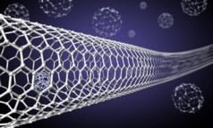
By achieving the synthesis of a novel nanohybrid structure by means of the pulsed laser ablation (PLA) technique, Professor My Ali El Khakani and his team paved the way for a new generation of optoelectronic materials. The combination of carbon nanotubes and lead sulfide (PbS) nanoparticles was performed using an effective and relatively simple process that offers considerable latitude for creating other nanohybrids for a variety of applications. The INRS Énergie Matériaux Télécommunications Research Centre researcher's work, published in the renowned journal Advanced Materials, presents very promising prospects for the development of third-generation solar devices, fast photodetectors, and optoelectronic switches.
INRS develops a nanohybrid with remarkable properties using a new laser-plasma process: Towards a new generation of optoelectronic nanomaterials
Montreal, Canada | Posted on January 25th, 2013In recent years, research on the photoelectronic properties of semiconductor nanoparticles, such as PbS, has been growing. The coupling of these nanoparticles with carbon nanotubes is a promising strategy for effectively generating photocurrent. The synthesis methods used by other research teams had significant limitations. "When chemically synthesizing nanohybrids, researchers used ligands, which prevented nanoparticle agglomeration, on one hand, but significantly affected the charge transfer dynamics from nanoparticles to nanotubes," said Professor El Khakani. Ligands reduce photoresponse efficiency and increase the reaction time—two effects that were not observed in nanohybrids produced by PLA since PbS is in direct atomic contact with the nanotubes' surafce.
"At the beginning, we didn't know if the nanohybrids would form in such a way as to enable their effective use for photodetection," said Ibrahima Ka, an INRS doctoral student working under the supervision of Professor El Khakani and co-supervised by Professor Dongling Ma. "By optimizing our approach, we developed nanohybrids whose photoactivity can be almost tailored at will." By integrating the new nanohybrid material into functional photoconductive devices, the researchers were pleased to demonstrate its strong photoresponse, which overpasses the results obtained by other methods. Thus, they have been able to achieve photoresponse values as high as 670% at 633 nm and 1350% at 405 nm under conditions where other nanohybrids did not exceed 37%. Furthermore, when the material is illuminated by a laser, the photocurrent response time is 1,000 to 100,000 times faster than those reported to date for other nanohybrids.
The PLA synthesis process produces very pure nanostructures and provides greater control over nanohybrid characteristics. Professor El Khakani's results demonstrate the enormous potential of these carbon nanotubes with PbS quantum dots.
Source: Stéphanie Thibault, Communications Advisor
####
About INRS
Institut national de recherche scientifique (INRS) is research intensive university which offers graduate level training. It ranks first in Canada for research intensity (average grant funding per faculty member). INRS brings together some 150 professors and close to 700 students and postdoctoral fellows at its four centres in Montreal, Quebec City, Laval, and Varennes. Its applied and fundamental research is essential to the advancement of science in Quebec and internationally, even as it plays a key role in the development of concrete solutions to the problems faced by our society.
About this publication
The article entitled "Pulsed Laser Ablation based Direct Synthesis of Single-Wall Carbon Nanotube/PbS Quantum Dot Nanohybrids Exhibiting Strong, Spectrally Wide and Fast Photoresponse" was published in the journal Advanced Materials on December 11, 2012, (Vol. 24, pp. 6289) and selected for the journal's frontispiece. The research of My Ali El Khakani, a professor and researcher at INRS's Énergie Matériaux Télécommunications Research Centre, was made possible by the financial support of the Natural Sciences and Engineering Research Council of Canada (NSERC) and the Fonds de recherche du Québec Nature and Technology fund, as well as support from Plasma-Québec's strategic network and Nano-Québec.
For more information, please click here
Contacts:
Stéphanie Thibault
Communications Advisor
Communications and Public Affairs Department
450-687-5010 x8865
Copyright © INRS
If you have a comment, please Contact us.Issuers of news releases, not 7th Wave, Inc. or Nanotechnology Now, are solely responsible for the accuracy of the content.
Bookmark:


| Related News Press |
News and information
![]() Simulating magnetization in a Heisenberg quantum spin chain April 5th, 2024
Simulating magnetization in a Heisenberg quantum spin chain April 5th, 2024
![]() NRL charters Navy’s quantum inertial navigation path to reduce drift April 5th, 2024
NRL charters Navy’s quantum inertial navigation path to reduce drift April 5th, 2024
![]() Discovery points path to flash-like memory for storing qubits: Rice find could hasten development of nonvolatile quantum memory April 5th, 2024
Discovery points path to flash-like memory for storing qubits: Rice find could hasten development of nonvolatile quantum memory April 5th, 2024
Nanotubes/Buckyballs/Fullerenes/Nanorods/Nanostrings
![]() Tests find no free-standing nanotubes released from tire tread wear September 8th, 2023
Tests find no free-standing nanotubes released from tire tread wear September 8th, 2023
![]() Detection of bacteria and viruses with fluorescent nanotubes July 21st, 2023
Detection of bacteria and viruses with fluorescent nanotubes July 21st, 2023
Optical computing/Photonic computing
![]() With VECSELs towards the quantum internet Fraunhofer: IAF achieves record output power with VECSEL for quantum frequency converters April 5th, 2024
With VECSELs towards the quantum internet Fraunhofer: IAF achieves record output power with VECSEL for quantum frequency converters April 5th, 2024
![]() Chemical reactions can scramble quantum information as well as black holes April 5th, 2024
Chemical reactions can scramble quantum information as well as black holes April 5th, 2024
![]() Optically trapped quantum droplets of light can bind together to form macroscopic complexes March 8th, 2024
Optically trapped quantum droplets of light can bind together to form macroscopic complexes March 8th, 2024
![]() HKUST researchers develop new integration technique for efficient coupling of III-V and silicon February 16th, 2024
HKUST researchers develop new integration technique for efficient coupling of III-V and silicon February 16th, 2024
Sensors
Discoveries
![]() Chemical reactions can scramble quantum information as well as black holes April 5th, 2024
Chemical reactions can scramble quantum information as well as black holes April 5th, 2024
![]() New micromaterial releases nanoparticles that selectively destroy cancer cells April 5th, 2024
New micromaterial releases nanoparticles that selectively destroy cancer cells April 5th, 2024
![]() Utilizing palladium for addressing contact issues of buried oxide thin film transistors April 5th, 2024
Utilizing palladium for addressing contact issues of buried oxide thin film transistors April 5th, 2024
Announcements
![]() NRL charters Navy’s quantum inertial navigation path to reduce drift April 5th, 2024
NRL charters Navy’s quantum inertial navigation path to reduce drift April 5th, 2024
![]() Discovery points path to flash-like memory for storing qubits: Rice find could hasten development of nonvolatile quantum memory April 5th, 2024
Discovery points path to flash-like memory for storing qubits: Rice find could hasten development of nonvolatile quantum memory April 5th, 2024
Energy
![]() Development of zinc oxide nanopagoda array photoelectrode: photoelectrochemical water-splitting hydrogen production January 12th, 2024
Development of zinc oxide nanopagoda array photoelectrode: photoelectrochemical water-splitting hydrogen production January 12th, 2024
![]() Shedding light on unique conduction mechanisms in a new type of perovskite oxide November 17th, 2023
Shedding light on unique conduction mechanisms in a new type of perovskite oxide November 17th, 2023
![]() Inverted perovskite solar cell breaks 25% efficiency record: Researchers improve cell efficiency using a combination of molecules to address different November 17th, 2023
Inverted perovskite solar cell breaks 25% efficiency record: Researchers improve cell efficiency using a combination of molecules to address different November 17th, 2023
![]() The efficient perovskite cells with a structured anti-reflective layer – another step towards commercialization on a wider scale October 6th, 2023
The efficient perovskite cells with a structured anti-reflective layer – another step towards commercialization on a wider scale October 6th, 2023
Quantum Dots/Rods
![]() A new kind of magnetism November 17th, 2023
A new kind of magnetism November 17th, 2023
![]() IOP Publishing celebrates World Quantum Day with the announcement of a special quantum collection and the winners of two prestigious quantum awards April 14th, 2023
IOP Publishing celebrates World Quantum Day with the announcement of a special quantum collection and the winners of two prestigious quantum awards April 14th, 2023
![]() Qubits on strong stimulants: Researchers find ways to improve the storage time of quantum information in a spin rich material January 27th, 2023
Qubits on strong stimulants: Researchers find ways to improve the storage time of quantum information in a spin rich material January 27th, 2023
![]() NIST’s grid of quantum islands could reveal secrets for powerful technologies November 18th, 2022
NIST’s grid of quantum islands could reveal secrets for powerful technologies November 18th, 2022
Photonics/Optics/Lasers
![]() With VECSELs towards the quantum internet Fraunhofer: IAF achieves record output power with VECSEL for quantum frequency converters April 5th, 2024
With VECSELs towards the quantum internet Fraunhofer: IAF achieves record output power with VECSEL for quantum frequency converters April 5th, 2024
![]() Nanoscale CL thermometry with lanthanide-doped heavy-metal oxide in TEM March 8th, 2024
Nanoscale CL thermometry with lanthanide-doped heavy-metal oxide in TEM March 8th, 2024
![]() Optically trapped quantum droplets of light can bind together to form macroscopic complexes March 8th, 2024
Optically trapped quantum droplets of light can bind together to form macroscopic complexes March 8th, 2024
![]() HKUST researchers develop new integration technique for efficient coupling of III-V and silicon February 16th, 2024
HKUST researchers develop new integration technique for efficient coupling of III-V and silicon February 16th, 2024
Solar/Photovoltaic
![]() Development of zinc oxide nanopagoda array photoelectrode: photoelectrochemical water-splitting hydrogen production January 12th, 2024
Development of zinc oxide nanopagoda array photoelectrode: photoelectrochemical water-splitting hydrogen production January 12th, 2024
![]() Shedding light on unique conduction mechanisms in a new type of perovskite oxide November 17th, 2023
Shedding light on unique conduction mechanisms in a new type of perovskite oxide November 17th, 2023
![]() Inverted perovskite solar cell breaks 25% efficiency record: Researchers improve cell efficiency using a combination of molecules to address different November 17th, 2023
Inverted perovskite solar cell breaks 25% efficiency record: Researchers improve cell efficiency using a combination of molecules to address different November 17th, 2023
![]() Charged “molecular beasts” the basis for new compounds: Researchers at Leipzig University use “aggressive” fragments of molecular ions for chemical synthesis November 3rd, 2023
Charged “molecular beasts” the basis for new compounds: Researchers at Leipzig University use “aggressive” fragments of molecular ions for chemical synthesis November 3rd, 2023
|
|
||
|
|
||
| The latest news from around the world, FREE | ||
|
|
||
|
|
||
| Premium Products | ||
|
|
||
|
Only the news you want to read!
Learn More |
||
|
|
||
|
Full-service, expert consulting
Learn More |
||
|
|
||