Home > Press > Self-assembling silica microwires may herald new generation of integrated optical devices: Optical Materials Express paper details new laser technique with applications in sensing, photovoltaics, optical switches
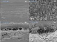 |
| These scanning electron microscope images reveal how UV laser light changes the surface texture and wettability of glass. Figures (a) and (b) reveal subtle texturing after lower-energy exposure to laser light. These textures made the surfaces more hydrophilic in (a) and more hydrophobic (water repellent) in (b). Higher energies produced a rougher and even more hydrophilic (wettable) (c) and (d) close-up of (c), surface.
Credit: Optical Materials Express. |
Abstract:
Silica microwires are the tiny and as-yet underutilized cousins of optical fibers. If precisely manufactured, however, these hair-like slivers of silica could enable applications and technology not currently possible with comparatively bulky optical fiber. By carefully controlling the shape of water droplets with an ultraviolet laser, a team of researchers from Australia and France has found a way to coax silica nanoparticles to self-assemble into much more highly uniform silica wires.
Self-assembling silica microwires may herald new generation of integrated optical devices: Optical Materials Express paper details new laser technique with applications in sensing, photovoltaics, optical switches
Washington, DC | Posted on January 25th, 2013The international team describes their novel manufacturing technique and its potential applications in a paper published today in the Optical Society's (OSA) open-access journal Optical Materials Express. This technique is particularly significant, according to the researchers, because it could, for the first time, enable silica to be combined with any material through a process of microwire self-assembly.
"We're currently living in the 'Glass Age,' based upon silica, which enables the Internet," says John Canning, team member and a professor in the school of chemistry at The University of Sydney in Australia. "Silica's high thermal processing, ruggedness, and unbeatable optical transparency over long distances equate to unprecedented capacity to transmit data and information all over the world."
Silica, however, is normally incompatible with most other materials so functionalizing silica (giving it the capability) to do more than just carry light has been a challenge. Further, bridging the gap between the light-speed transmission of data through silica and electronic and photonic components - such as optical switches, optical circuits, photon sources, and even sensors - requires some form of interconnect. But this transition is highly inefficient using optical fibers and interconnection losses remain one of the largest unresolved issues in optical communications.
Silica microwires, if they could be manufactured or self-assembled in place, have the potential to operate as optical interconnects. They also could achieve new functionality by adding different chemicals that can only be introduced by self-assembly.
Silica wires, unlike optical fiber, have no cladding, which means greater confinement of light in a smaller structure better suited for interconnection, further minimizing losses and physical space. "So we were motivated to solve the great silica incompatibility problem," explains Canning.
To this end, the researchers came up with the idea of using evaporative self-assembly of silica nanoparticles at room temperature. They recently reported this breakthrough in the journal Nature Communications, demonstrating single-photon-emitting nanodiamonds embedded in silica, which is a first step toward a practical photon source for future quantum computing.
The key to carrying this innovation further, as described in their new research published today in Optical Materials Express, is perfecting the manufacturing process so highly uniform wires self-assemble from nanoparticles suspended in a solution. The challenge has been that as naturally forming round droplets evaporate, they produce very uneven silica microwires. This is due to the microfluidic currents inside the droplet, which corral the nanoparticles into specific patterns aided and held together by intermolecular attractive forces. The nanoparticles then crystalize when the solvent (water) evaporates.
Canning and his team realized that by changing the shape of the droplet and elongating it ever so slightly, they could concurrently change the flow patterns inside the drop, controlling how the nanoparticles assemble.
The researchers did this by changing the "wettability" properties of the glass the drops were resting upon. The team used an ultraviolet laser to alter and pattern a glass made of the mineral borosilicate. This patterning made the surface more wettable in a very controlled way, allowing the droplet to assume a slightly more oblong shape. This subtle shape change was enough to alter the microscopic flows and eddies so as the water evaporated, the silica formed straighter, more uniform microwires.
The researchers anticipate that their processing technology will allow complete control of nanoparticle self-assembly for various technologies, including microwire devices and sensors, photon sources, and possibly silica-based integrated circuits.
It also will enable the production of selective devices such as chemical and biological sensors, photovoltaic structures, and novel switches in both optical fiber form and on waveguides - all of which could lead to technologies that seamlessly integrate microfluidic, electronic, quantum, and photonic functionality.
####
About Optical Society of America
Uniting more than 180,000 professionals from 175 countries, the Optical Society (OSA) brings together the global optics community through its programs and initiatives. Since 1916 OSA has worked to advance the common interests of the field, providing educational resources to the scientists, engineers and business leaders who work in the field by promoting the science of light and the advanced technologies made possible by optics and photonics. OSA publications, events, technical groups and programs foster optics knowledge and scientific collaboration among all those with an interest in optics and photonics. For more information, visit www.osa.org.
About Optical Materials Express
Optical Materials Express (OMEx) is OSA's newest peer-reviewed, open-access journal focusing on the synthesis, processing and characterization of materials for applications in optics and photonics. OMEx primarily emphasizes advances in novel optical materials, their properties, modeling, synthesis and fabrication techniques; how such materials contribute to novel optical behavior; and how they enable new or improved optical devices. It is published by the Optical Society and edited by David J. Hagan of the University of Central Florida. For more information, visit www.OpticsInfoBase.org/OMEx.
For more information, please click here
Contacts:
Brielle Day
202-416-1435
Copyright © Optical Society of America
If you have a comment, please Contact us.Issuers of news releases, not 7th Wave, Inc. or Nanotechnology Now, are solely responsible for the accuracy of the content.
Bookmark:


| Related Links |
| Related News Press |
News and information
![]() Simulating magnetization in a Heisenberg quantum spin chain April 5th, 2024
Simulating magnetization in a Heisenberg quantum spin chain April 5th, 2024
![]() NRL charters Navy�s quantum inertial navigation path to reduce drift April 5th, 2024
NRL charters Navy�s quantum inertial navigation path to reduce drift April 5th, 2024
![]() Discovery points path to flash-like memory for storing qubits: Rice find could hasten development of nonvolatile quantum memory April 5th, 2024
Discovery points path to flash-like memory for storing qubits: Rice find could hasten development of nonvolatile quantum memory April 5th, 2024
Chip Technology
![]() Discovery points path to flash-like memory for storing qubits: Rice find could hasten development of nonvolatile quantum memory April 5th, 2024
Discovery points path to flash-like memory for storing qubits: Rice find could hasten development of nonvolatile quantum memory April 5th, 2024
![]() Utilizing palladium for addressing contact issues of buried oxide thin film transistors April 5th, 2024
Utilizing palladium for addressing contact issues of buried oxide thin film transistors April 5th, 2024
![]() HKUST researchers develop new integration technique for efficient coupling of III-V and silicon February 16th, 2024
HKUST researchers develop new integration technique for efficient coupling of III-V and silicon February 16th, 2024
Self Assembly
![]() Liquid crystal templated chiral nanomaterials October 14th, 2022
Liquid crystal templated chiral nanomaterials October 14th, 2022
![]() Nanoclusters self-organize into centimeter-scale hierarchical assemblies April 22nd, 2022
Nanoclusters self-organize into centimeter-scale hierarchical assemblies April 22nd, 2022
![]() Atom by atom: building precise smaller nanoparticles with templates March 4th, 2022
Atom by atom: building precise smaller nanoparticles with templates March 4th, 2022
![]() Nanostructures get complex with electron equivalents: Nanoparticles of two different sizes break away from symmetrical designs January 14th, 2022
Nanostructures get complex with electron equivalents: Nanoparticles of two different sizes break away from symmetrical designs January 14th, 2022
Optical computing/Photonic computing
![]() With VECSELs towards the quantum internet Fraunhofer: IAF achieves record output power with VECSEL for quantum frequency converters April 5th, 2024
With VECSELs towards the quantum internet Fraunhofer: IAF achieves record output power with VECSEL for quantum frequency converters April 5th, 2024
![]() Chemical reactions can scramble quantum information as well as black holes April 5th, 2024
Chemical reactions can scramble quantum information as well as black holes April 5th, 2024
![]() Optically trapped quantum droplets of light can bind together to form macroscopic complexes March 8th, 2024
Optically trapped quantum droplets of light can bind together to form macroscopic complexes March 8th, 2024
![]() HKUST researchers develop new integration technique for efficient coupling of III-V and silicon February 16th, 2024
HKUST researchers develop new integration technique for efficient coupling of III-V and silicon February 16th, 2024
Sensors
Discoveries
![]() Chemical reactions can scramble quantum information as well as black holes April 5th, 2024
Chemical reactions can scramble quantum information as well as black holes April 5th, 2024
![]() New micromaterial releases nanoparticles that selectively destroy cancer cells April 5th, 2024
New micromaterial releases nanoparticles that selectively destroy cancer cells April 5th, 2024
![]() Utilizing palladium for addressing contact issues of buried oxide thin film transistors April 5th, 2024
Utilizing palladium for addressing contact issues of buried oxide thin film transistors April 5th, 2024
Announcements
![]() NRL charters Navy�s quantum inertial navigation path to reduce drift April 5th, 2024
NRL charters Navy�s quantum inertial navigation path to reduce drift April 5th, 2024
![]() Discovery points path to flash-like memory for storing qubits: Rice find could hasten development of nonvolatile quantum memory April 5th, 2024
Discovery points path to flash-like memory for storing qubits: Rice find could hasten development of nonvolatile quantum memory April 5th, 2024
Energy
![]() Development of zinc oxide nanopagoda array photoelectrode: photoelectrochemical water-splitting hydrogen production January 12th, 2024
Development of zinc oxide nanopagoda array photoelectrode: photoelectrochemical water-splitting hydrogen production January 12th, 2024
![]() Shedding light on unique conduction mechanisms in a new type of perovskite oxide November 17th, 2023
Shedding light on unique conduction mechanisms in a new type of perovskite oxide November 17th, 2023
![]() Inverted perovskite solar cell breaks 25% efficiency record: Researchers improve cell efficiency using a combination of molecules to address different November 17th, 2023
Inverted perovskite solar cell breaks 25% efficiency record: Researchers improve cell efficiency using a combination of molecules to address different November 17th, 2023
![]() The efficient perovskite cells with a structured anti-reflective layer � another step towards commercialization on a wider scale October 6th, 2023
The efficient perovskite cells with a structured anti-reflective layer � another step towards commercialization on a wider scale October 6th, 2023
Photonics/Optics/Lasers
![]() With VECSELs towards the quantum internet Fraunhofer: IAF achieves record output power with VECSEL for quantum frequency converters April 5th, 2024
With VECSELs towards the quantum internet Fraunhofer: IAF achieves record output power with VECSEL for quantum frequency converters April 5th, 2024
![]() Nanoscale CL thermometry with lanthanide-doped heavy-metal oxide in TEM March 8th, 2024
Nanoscale CL thermometry with lanthanide-doped heavy-metal oxide in TEM March 8th, 2024
![]() Optically trapped quantum droplets of light can bind together to form macroscopic complexes March 8th, 2024
Optically trapped quantum droplets of light can bind together to form macroscopic complexes March 8th, 2024
![]() HKUST researchers develop new integration technique for efficient coupling of III-V and silicon February 16th, 2024
HKUST researchers develop new integration technique for efficient coupling of III-V and silicon February 16th, 2024
Solar/Photovoltaic
![]() Development of zinc oxide nanopagoda array photoelectrode: photoelectrochemical water-splitting hydrogen production January 12th, 2024
Development of zinc oxide nanopagoda array photoelectrode: photoelectrochemical water-splitting hydrogen production January 12th, 2024
![]() Shedding light on unique conduction mechanisms in a new type of perovskite oxide November 17th, 2023
Shedding light on unique conduction mechanisms in a new type of perovskite oxide November 17th, 2023
![]() Inverted perovskite solar cell breaks 25% efficiency record: Researchers improve cell efficiency using a combination of molecules to address different November 17th, 2023
Inverted perovskite solar cell breaks 25% efficiency record: Researchers improve cell efficiency using a combination of molecules to address different November 17th, 2023
![]() Charged �molecular beasts� the basis for new compounds: Researchers at Leipzig University use �aggressive� fragments of molecular ions for chemical synthesis November 3rd, 2023
Charged �molecular beasts� the basis for new compounds: Researchers at Leipzig University use �aggressive� fragments of molecular ions for chemical synthesis November 3rd, 2023
|
|
||
|
|
||
| The latest news from around the world, FREE | ||
|
|
||
|
|
||
| Premium Products | ||
|
|
||
|
Only the news you want to read!
Learn More |
||
|
|
||
|
Full-service, expert consulting
Learn More |
||
|
|
||