Home > Press > Quantum Communication: Each Photon Counts: Emmy Noether Research Group Leader Wolfram Pernice Achieves Breakthrough at KIT in Building an Efficient Single-photon Detector
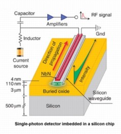 |
| The single-photon detector is characterized by five convincing factors: 91% detection efficiency; direct integration on chip; counting rates on a Gigahertz scale; high timing resolution and negligible dark counting rates. Source: KIT/CFN |
Abstract:
Ultrafast, efficient, and reliable single-photon detectors are among the most sought-after components in photonics and quantum communication, which have not yet reached maturity for practical application. Physicist Dr. Wolfram Pernice of the Karlsruhe Institute of Technology (KIT), in cooperation with colleagues at Yale University, Boston University, and Moscow State Pedagogical University, achieved the decisive breakthrough by integrating single-photon detectors with nanophotonic chips. The detector combines near-unity detection efficiency with high timing resolution and has a very low error rate. The results have been published by Nature Communications (doi:10.1038/ncomms2307).
Quantum Communication: Each Photon Counts: Emmy Noether Research Group Leader Wolfram Pernice Achieves Breakthrough at KIT in Building an Efficient Single-photon Detector
Germany | Posted on January 25th, 2013Without reliable detection of single photons, it is impossible to make real use of the latest advances in optical data transmission or quantum computation; it is like having no analog-digital converter in a conventional computer to determine whether the applied voltage stands for 0 or 1. Although a number of different single-photon detector models have been developed over the past few years, thus far, none have provided satisfactory performance.
Several new ideas and advanced developments went into the prototype developed within the "Integrated Quantum Photonics" project at the DFG Center of Functional Nanostructures (CFN). The new single-photon detector, tested in the telecommunications wavelength range, achieves a previously unattained detection efficiency of 91%.
The detector was realized by fabricating superconducting nanowires directly on top of a nanophotonic waveguide. This geometry can be compared to a tube that conducts light, around which a wire in a superconducting state is wound and, as such, has no electric resistivity. The nanometer-sized wire made of niobium nitride absorbs photons that propagate along the waveguide. When a photon is absorbed, superconductivity is lost, which is detected as an electric signal. The longer the tube, the higher is the detection probability. The lengths involved are in the micrometer range.
A special feature of the detector is its direct installation on the chip, which allows for it to be replicated at random. The single-photon detectors built thus far were stand-alone units, which were connected to chips with optical fibers. Arrangements of that type suffer from photons being lost in the fiber connection or being absorbed in other ways. These loss channels do not exist in the detector that is now fully embedded in a silicon photonic circuit. In addition to high detection efficiency, this gives rise to a remarkably low dark count rate. Dark counts arise when a photon is detected erroneously: for instance, because of a spontaneous emission, an alpha particle, or a spurious field. The new design also provides ultrashort timing jitter of 18 picoseconds, which is 18 times 10-12 seconds.
The novel solution also makes it possible to integrate several hundreds of these detectors on a single chip. This is a basic precondition for future use in optical quantum computers.
The detector demonstrated in this study was designed to work at wavelengths in the Telekom bandwidth. The same detector architecture can also be used for wavelengths in the range of visible light. This would allow the principle to be employed in analyses of all structures that emit little light, i.e., photons, such as single molecules or bacteria.
####
About Helmholtz Association of German Research Centres
The Helmholtz Association is dedicated to pursuing the long-term research goals of state and society, and to maintaining and improving the livelihoods of the population. In order to do this, the Helmholtz Association carries out top-level research to identify and explore the major challenges facing society, science and the economy. Its work is divided into six strategic research fields: Energy; Earth and Environment; Health; Key Technologies; Structure of Matter; and Aeronautics, Space and Transport. The Helmholtz Association brings together 18 scientific-technical and biological-medical research centres. With some 32,698 employees and an annual budget of approximately �3.4 billion, the Helmholtz Association is Germany�s largest scientific organisation. Its work follows in the tradition of the great natural scientist Hermann von Helmholtz (1821-1894).
About Dr. Wolfram Pernice
Dr. Wolfram Pernice studied Microsystems Technology at Albert Ludwig University in Freiburg. After winning a research grant of the British Engineering and Physical Sciences Research Council he obtained his Ph.D. at the University of Oxford, England where he explored the Development of Efficient Numerical Methods for Simulating Photonic Devices. In 2008 he joined Yale University where, supported by a Humboldt scholarship, he analyzed nano-opto-mechanical systems in the group of Hong Tang. In summer 2011, the German Research Association (DFG) appointed him as head of an Emmy Noether Research Group. His research into integrated quantum optical and nano-opto-mechanical systems had convinced the committee, and as the recipient of an Emmy Noether grant, he chose to pursue his work at the Karlsruhe Institute of Technology (KIT). Since October 2011, he has worked here as a Junior Group Leader at the Institute of Nanotechnology (INT). At the beginning of the year, he also won a Helmholtz International Research Group grant, which he wants to use to fund another post-graduate student in his Karlsruhe team.
About The DFG Center of Functional Nanostructures (CFN)
The DFG Center of Functional Nanostructures (CFN) devotes its attention to the important area of nanotechnology and functional nanostructures. Its objective is to carry out excellent interdisciplinary and international research in order to produce nanostructures with new technical functions and take the first step from fundamental research to application. At the present time, more than 250 scientists and engineers cooperate in more than 80 sub-projects networked through the CFN in Karlsruhe, focusing on the areas of nano-photonics, nano-electronics, molecular nanostructures, nano-biology, and nano-energy. www.cfn.kit.edu
About Karlsruhe Institute of Technology (KIT)
Karlsruhe Institute of Technology (KIT) is a public corporation according to the legislation of the state of Baden-W�rttemberg. It fulfills the mission of a university and the mission of a national research center of the Helmholtz Association. KIT focuses on a knowledge triangle that links the tasks of research, teaching, and innovation.
For more information, please click here
Contacts:
Monika Landgraf
49-721-608-47414
Tatjana Erkert
DFG-Centrum f�r Funktionelle Nanostrukturen (CFN)
www.cfn.kit.edu
Tel.: +49 721 608-43409
Fax: +49 721 608-48496
tatjana erkert∂kit edu
Copyright © Helmholtz Association of German Research Centres
If you have a comment, please Contact us.Issuers of news releases, not 7th Wave, Inc. or Nanotechnology Now, are solely responsible for the accuracy of the content.
Bookmark:


| Related News Press |
News and information
![]() Simulating magnetization in a Heisenberg quantum spin chain April 5th, 2024
Simulating magnetization in a Heisenberg quantum spin chain April 5th, 2024
![]() NRL charters Navy�s quantum inertial navigation path to reduce drift April 5th, 2024
NRL charters Navy�s quantum inertial navigation path to reduce drift April 5th, 2024
![]() Discovery points path to flash-like memory for storing qubits: Rice find could hasten development of nonvolatile quantum memory April 5th, 2024
Discovery points path to flash-like memory for storing qubits: Rice find could hasten development of nonvolatile quantum memory April 5th, 2024
Laboratories
![]() A battery�s hopping ions remember where they�ve been: Seen in atomic detail, the seemingly smooth flow of ions through a battery�s electrolyte is surprisingly complicated February 16th, 2024
A battery�s hopping ions remember where they�ve been: Seen in atomic detail, the seemingly smooth flow of ions through a battery�s electrolyte is surprisingly complicated February 16th, 2024
![]() NRL discovers two-dimensional waveguides February 16th, 2024
NRL discovers two-dimensional waveguides February 16th, 2024
![]() Three-pronged approach discerns qualities of quantum spin liquids November 17th, 2023
Three-pronged approach discerns qualities of quantum spin liquids November 17th, 2023
Quantum Computing
![]() Simulating magnetization in a Heisenberg quantum spin chain April 5th, 2024
Simulating magnetization in a Heisenberg quantum spin chain April 5th, 2024
![]() Discovery points path to flash-like memory for storing qubits: Rice find could hasten development of nonvolatile quantum memory April 5th, 2024
Discovery points path to flash-like memory for storing qubits: Rice find could hasten development of nonvolatile quantum memory April 5th, 2024
![]() With VECSELs towards the quantum internet Fraunhofer: IAF achieves record output power with VECSEL for quantum frequency converters April 5th, 2024
With VECSELs towards the quantum internet Fraunhofer: IAF achieves record output power with VECSEL for quantum frequency converters April 5th, 2024
![]() Chemical reactions can scramble quantum information as well as black holes April 5th, 2024
Chemical reactions can scramble quantum information as well as black holes April 5th, 2024
Discoveries
![]() Chemical reactions can scramble quantum information as well as black holes April 5th, 2024
Chemical reactions can scramble quantum information as well as black holes April 5th, 2024
![]() New micromaterial releases nanoparticles that selectively destroy cancer cells April 5th, 2024
New micromaterial releases nanoparticles that selectively destroy cancer cells April 5th, 2024
![]() Utilizing palladium for addressing contact issues of buried oxide thin film transistors April 5th, 2024
Utilizing palladium for addressing contact issues of buried oxide thin film transistors April 5th, 2024
Announcements
![]() NRL charters Navy�s quantum inertial navigation path to reduce drift April 5th, 2024
NRL charters Navy�s quantum inertial navigation path to reduce drift April 5th, 2024
![]() Discovery points path to flash-like memory for storing qubits: Rice find could hasten development of nonvolatile quantum memory April 5th, 2024
Discovery points path to flash-like memory for storing qubits: Rice find could hasten development of nonvolatile quantum memory April 5th, 2024
Photonics/Optics/Lasers
![]() With VECSELs towards the quantum internet Fraunhofer: IAF achieves record output power with VECSEL for quantum frequency converters April 5th, 2024
With VECSELs towards the quantum internet Fraunhofer: IAF achieves record output power with VECSEL for quantum frequency converters April 5th, 2024
![]() Nanoscale CL thermometry with lanthanide-doped heavy-metal oxide in TEM March 8th, 2024
Nanoscale CL thermometry with lanthanide-doped heavy-metal oxide in TEM March 8th, 2024
![]() Optically trapped quantum droplets of light can bind together to form macroscopic complexes March 8th, 2024
Optically trapped quantum droplets of light can bind together to form macroscopic complexes March 8th, 2024
![]() HKUST researchers develop new integration technique for efficient coupling of III-V and silicon February 16th, 2024
HKUST researchers develop new integration technique for efficient coupling of III-V and silicon February 16th, 2024
Research partnerships
![]() Discovery points path to flash-like memory for storing qubits: Rice find could hasten development of nonvolatile quantum memory April 5th, 2024
Discovery points path to flash-like memory for storing qubits: Rice find could hasten development of nonvolatile quantum memory April 5th, 2024
![]() Researchers� approach may protect quantum computers from attacks March 8th, 2024
Researchers� approach may protect quantum computers from attacks March 8th, 2024
![]() 'Sudden death' of quantum fluctuations defies current theories of superconductivity: Study challenges the conventional wisdom of superconducting quantum transitions January 12th, 2024
'Sudden death' of quantum fluctuations defies current theories of superconductivity: Study challenges the conventional wisdom of superconducting quantum transitions January 12th, 2024
Quantum nanoscience
![]() Simulating magnetization in a Heisenberg quantum spin chain April 5th, 2024
Simulating magnetization in a Heisenberg quantum spin chain April 5th, 2024
![]() Optically trapped quantum droplets of light can bind together to form macroscopic complexes March 8th, 2024
Optically trapped quantum droplets of light can bind together to form macroscopic complexes March 8th, 2024
![]() Bridging light and electrons January 12th, 2024
Bridging light and electrons January 12th, 2024
![]() 'Sudden death' of quantum fluctuations defies current theories of superconductivity: Study challenges the conventional wisdom of superconducting quantum transitions January 12th, 2024
'Sudden death' of quantum fluctuations defies current theories of superconductivity: Study challenges the conventional wisdom of superconducting quantum transitions January 12th, 2024
|
|
||
|
|
||
| The latest news from around the world, FREE | ||
|
|
||
|
|
||
| Premium Products | ||
|
|
||
|
Only the news you want to read!
Learn More |
||
|
|
||
|
Full-service, expert consulting
Learn More |
||
|
|
||