Home > Press > Imec Teams With Cadence to Present Automated Design-for-Test (DFT) Solution for 3D Memory-on-Logic
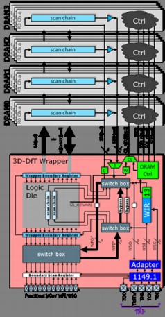 |
| Imec’s 3D wrapper extension for Wide-I/O DRAM |
Abstract:
At the European 3D TSV Summit in Grenoble, France on January 22-23, 2013, imec, a world-leading nano-electronics research institute, today announced that together with Cadence Design Systems they have developed, implemented and validated an automated 3D Design-for-Test (DFT) solution to test logic-memory interconnects in DRAM-on-logic stacks. The solution, based on Cadence® Encounter® Test technology, was verified on an industrial test chip containing a logic die and a JEDEC-compliant Wide-I/O Mobile DRAM.
Imec Teams With Cadence to Present Automated Design-for-Test (DFT) Solution for 3D Memory-on-Logic
Leuven, Belgium | Posted on January 22nd, 2013Memory-on-logic 3D stacks offer the possibility of heterogeneous integration with dense low-power inter-die interconnects. Hence, they are amongst the first 3D products that will come on the market, enabling next-generation high-performance low-power mobile applications. Recently, JEDEC has released a standard (JESD-229) for stackable Wide-I/O mobile dynamic random access memories (DRAMs) specifying the logic-memory interface. Unlike many previous DRAMs, the standard contains boundary scan features to facilitate interconnect testing. Imec and Cadence now present a design-for-test (DFT) architecture and corresponding automatic test pattern generation (ATPG) approach. It is an extension of their previously announced logic-on-logic 3D DFT architecture and it supports post-bond testing of the interconnects between the logic die and the DRAM stacked on top of it.
The solution implemented by Cadence and imec includes the generation of DRAM test control signals in the logic die and the inclusion of the DRAM boundary scan registers in the serial and parallel test access mechanisms (TAMs) of the 3D test architecture. The automated design for test solution has been validated on an industrial test chip. The design of the test chip is an interposer-based 3D stacked IC which includes a silicon interposer base die, a 94mm2 logic system-on-chip in 40nm technology, and a single Wide-I/O DRAM rank. The validation results show that the silicon area of the additional DFT wrapper is negligible compared to the total logic die size (<0.03%). Moreover, the test pattern generation was very efficient (tens of patterns, generated in only a few seconds) and effective (100% coverage of the targeted faults). All 3D-DFT logic in the logic die was automatically inserted with Cadence Encounter RTL Compiler while the Interconnect test patterns were generated with Encounter Test ATPG.
"This 3D memory-on-logic DFT solution is another big step forward toward market introduction of 3D-stacked IC for next-generation high-performance, low-power mobile applications," said Bassilios Petrakis, product marketing director for the Encounter Test product family at Cadence. "Our collaboration with imec has enabled the creation of an industry-leading solution that enhances efficiencies of 3D-IC design for our customers."
"Teaming up with Cadence enables us to automate the insertion of our DFT circuitry in a given design, and to automate the interconnect test pattern generation. Such automated flows make our technology valuable for the industry. We are confident that we can also handle the DFT features that start to emerge in other 3D memory standards," said Erik Jan Marinissen, Principal Scientist at imec.
Part of the work has been performed in the project ESiP, which is co-funded by the ENIAC Joint Undertaking.
####
About IMEC
Imec performs world-leading research in nano-electronics. Imec leverages its scientific knowledge with the innovative power of its global partnerships in ICT, healthcare and energy. Imec delivers industry-relevant technology solutions. In a unique high-tech environment, its international top talent is committed to providing the building blocks for a better life in a sustainable society. Imec is headquartered in Leuven, Belgium, and has offices in Belgium, the Netherlands, Taiwan, US, China, India and Japan. Its staff of close to 2,000 people includes more than 600 industrial residents and guest researchers. In 2011, imec's revenue (P&L) was about 300 million euro. Further information on imec can be found at www.imec.be.
Imec is a registered trademark for the activities of IMEC International (a legal entity set up under Belgian law as a "stichting van openbaar nut”), imec Belgium (IMEC vzw supported by the Flemish Government), imec the Netherlands (Stichting IMEC Nederland, part of Holst Centre which is supported by the Dutch Government), imec Taiwan (IMEC Taiwan Co.) and imec China (IMEC Microelectronics (Shangai) Co. Ltd.) and imec India (Imec India Private Limited).
For more information, please click here
Contacts:
Hanne Degans
External Communications Officer
T: +32 16 28 17 69
Mobile: +32 486 065 175
Olga Walsh | Business Technology
[ f o r m u l a ]
Formula PR, Inc.
1215 Cushman Avenue
San Diego, CA 92110
Office 619-234-0345 |
Copyright © IMEC
If you have a comment, please Contact us.Issuers of news releases, not 7th Wave, Inc. or Nanotechnology Now, are solely responsible for the accuracy of the content.
Bookmark:


| Related News Press |
News and information
![]() Simulating magnetization in a Heisenberg quantum spin chain April 5th, 2024
Simulating magnetization in a Heisenberg quantum spin chain April 5th, 2024
![]() NRL charters Navy’s quantum inertial navigation path to reduce drift April 5th, 2024
NRL charters Navy’s quantum inertial navigation path to reduce drift April 5th, 2024
![]() Discovery points path to flash-like memory for storing qubits: Rice find could hasten development of nonvolatile quantum memory April 5th, 2024
Discovery points path to flash-like memory for storing qubits: Rice find could hasten development of nonvolatile quantum memory April 5th, 2024
Chip Technology
![]() Discovery points path to flash-like memory for storing qubits: Rice find could hasten development of nonvolatile quantum memory April 5th, 2024
Discovery points path to flash-like memory for storing qubits: Rice find could hasten development of nonvolatile quantum memory April 5th, 2024
![]() Utilizing palladium for addressing contact issues of buried oxide thin film transistors April 5th, 2024
Utilizing palladium for addressing contact issues of buried oxide thin film transistors April 5th, 2024
![]() HKUST researchers develop new integration technique for efficient coupling of III-V and silicon February 16th, 2024
HKUST researchers develop new integration technique for efficient coupling of III-V and silicon February 16th, 2024
Memory Technology
![]() Utilizing palladium for addressing contact issues of buried oxide thin film transistors April 5th, 2024
Utilizing palladium for addressing contact issues of buried oxide thin film transistors April 5th, 2024
![]() Interdisciplinary: Rice team tackles the future of semiconductors Multiferroics could be the key to ultralow-energy computing October 6th, 2023
Interdisciplinary: Rice team tackles the future of semiconductors Multiferroics could be the key to ultralow-energy computing October 6th, 2023
![]() Researchers discover materials exhibiting huge magnetoresistance June 9th, 2023
Researchers discover materials exhibiting huge magnetoresistance June 9th, 2023
Announcements
![]() NRL charters Navy’s quantum inertial navigation path to reduce drift April 5th, 2024
NRL charters Navy’s quantum inertial navigation path to reduce drift April 5th, 2024
![]() Discovery points path to flash-like memory for storing qubits: Rice find could hasten development of nonvolatile quantum memory April 5th, 2024
Discovery points path to flash-like memory for storing qubits: Rice find could hasten development of nonvolatile quantum memory April 5th, 2024
Events/Classes
![]() Researchers demonstrate co-propagation of quantum and classical signals: Study shows that quantum encryption can be implemented in existing fiber networks January 20th, 2023
Researchers demonstrate co-propagation of quantum and classical signals: Study shows that quantum encryption can be implemented in existing fiber networks January 20th, 2023
Alliances/Trade associations/Partnerships/Distributorships
![]() Chicago Quantum Exchange welcomes six new partners highlighting quantum technology solutions, from Chicago and beyond September 23rd, 2022
Chicago Quantum Exchange welcomes six new partners highlighting quantum technology solutions, from Chicago and beyond September 23rd, 2022
![]() University of Illinois Chicago joins Brookhaven Lab's Quantum Center June 10th, 2022
University of Illinois Chicago joins Brookhaven Lab's Quantum Center June 10th, 2022
|
|
||
|
|
||
| The latest news from around the world, FREE | ||
|
|
||
|
|
||
| Premium Products | ||
|
|
||
|
Only the news you want to read!
Learn More |
||
|
|
||
|
Full-service, expert consulting
Learn More |
||
|
|
||