Home > Press > Researchers Develop Integrated Dual-mode Active and Passive Infrared Camera: Based on type-II superlattices, high-performance infrared camera could aid search-and-rescue missions
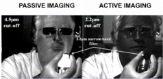 |
| A Center for Quantum Devices researcher holds a heater and a narrow-band filter centered at 3.6�m. The heater can be seen when imaged with the band-pass detectors sensitive up to 4.5�m (left), but not in the ones with shorter detection wavelengths up to 2.2�m (right). |
Abstract:
High-performance infrared cameras are crucial for civilian and military applications such as night-vision goggles and search-and-rescue operations. Existing cameras usually fall into one of two types: active cameras, which use an invisible infrared source to illuminate the scene, usually in the near or short-wavelength infrared; and passive cameras, which detect the thermal radiation given off by a warm object, typically in the mid- or long-wavelength infrared, without the need for any illumination. Both camera types have advantages and disadvantages in the field.
Researchers Develop Integrated Dual-mode Active and Passive Infrared Camera: Based on type-II superlattices, high-performance infrared camera could aid search-and-rescue missions
Chicago, IL | Posted on January 16th, 2013Integrating both modes of imaging into a single camera would open new possibilities � but doing so has proven challenging. Until now, dual-mode active and passive infrared cameras needed either two different infrared detectors or complex controllable filters to accommodate the different wavelengths, and then required additional signal processing to reconstruct a single image from the two modes.
However, in a move that may change the way we look a two-color imaging, researchers at the Northwestern University's Center for Quantum Devices have now found a way to integrate active and passive infrared imaging capability into a single chip. This opens the way to lighter and simpler dual-mode active/passive cameras with lower power dissipation.
A paper about the findings, "Active and Passive Infrared Imager Based on Short-Wave and Mid-Wave Type-II Superlattice Dual-Band Detectors," was published January 1 in the journal Optic Letters. The work was led by Manijeh Razeghi, Walter P. Murphy Professor of Electrical Engineering and Computer Science in Northwestern's McCormick School of Engineering and Applied Science.
The researchers achieved this feat by engineering the quantum properties of novel semiconductor materials called the indium arsenide/gallium antimonide (InAs/GaSb) type-II superlattices. Researchers at the center have been pioneering the development of type-II superlattices as a superior replacement of aging mercury-cadmium-telluride (HgCdTe) infrared camera technology in terms of both performance and cost.
Using the unique band-structure engineering capabilities of type-II superlattices, they have developed a new structure incorporating two different superlattices with different layer spacings, thus enabling detection with a cutoff wavelength of either 2.2�m (active mode) or 4.5�m (passive mode). This new device can simply switch from passive to active mode by a very small change in bias.
The work was funded by the Defense Advanced Research Projects Agency.
####
For more information, please click here
Contacts:
Megan Fellman
847-491-3115
Copyright © Northwestern University
If you have a comment, please Contact us.Issuers of news releases, not 7th Wave, Inc. or Nanotechnology Now, are solely responsible for the accuracy of the content.
Bookmark:


| Related News Press |
News and information
![]() Simulating magnetization in a Heisenberg quantum spin chain April 5th, 2024
Simulating magnetization in a Heisenberg quantum spin chain April 5th, 2024
![]() NRL charters Navy�s quantum inertial navigation path to reduce drift April 5th, 2024
NRL charters Navy�s quantum inertial navigation path to reduce drift April 5th, 2024
![]() Discovery points path to flash-like memory for storing qubits: Rice find could hasten development of nonvolatile quantum memory April 5th, 2024
Discovery points path to flash-like memory for storing qubits: Rice find could hasten development of nonvolatile quantum memory April 5th, 2024
Govt.-Legislation/Regulation/Funding/Policy
![]() NRL charters Navy�s quantum inertial navigation path to reduce drift April 5th, 2024
NRL charters Navy�s quantum inertial navigation path to reduce drift April 5th, 2024
![]() Discovery points path to flash-like memory for storing qubits: Rice find could hasten development of nonvolatile quantum memory April 5th, 2024
Discovery points path to flash-like memory for storing qubits: Rice find could hasten development of nonvolatile quantum memory April 5th, 2024
![]() Chemical reactions can scramble quantum information as well as black holes April 5th, 2024
Chemical reactions can scramble quantum information as well as black holes April 5th, 2024
Discoveries
![]() Chemical reactions can scramble quantum information as well as black holes April 5th, 2024
Chemical reactions can scramble quantum information as well as black holes April 5th, 2024
![]() New micromaterial releases nanoparticles that selectively destroy cancer cells April 5th, 2024
New micromaterial releases nanoparticles that selectively destroy cancer cells April 5th, 2024
![]() Utilizing palladium for addressing contact issues of buried oxide thin film transistors April 5th, 2024
Utilizing palladium for addressing contact issues of buried oxide thin film transistors April 5th, 2024
Announcements
![]() NRL charters Navy�s quantum inertial navigation path to reduce drift April 5th, 2024
NRL charters Navy�s quantum inertial navigation path to reduce drift April 5th, 2024
![]() Discovery points path to flash-like memory for storing qubits: Rice find could hasten development of nonvolatile quantum memory April 5th, 2024
Discovery points path to flash-like memory for storing qubits: Rice find could hasten development of nonvolatile quantum memory April 5th, 2024
Military
![]() NRL charters Navy�s quantum inertial navigation path to reduce drift April 5th, 2024
NRL charters Navy�s quantum inertial navigation path to reduce drift April 5th, 2024
![]() What heat can tell us about battery chemistry: using the Peltier effect to study lithium-ion cells March 8th, 2024
What heat can tell us about battery chemistry: using the Peltier effect to study lithium-ion cells March 8th, 2024
![]() New chip opens door to AI computing at light speed February 16th, 2024
New chip opens door to AI computing at light speed February 16th, 2024
Photonics/Optics/Lasers
![]() With VECSELs towards the quantum internet Fraunhofer: IAF achieves record output power with VECSEL for quantum frequency converters April 5th, 2024
With VECSELs towards the quantum internet Fraunhofer: IAF achieves record output power with VECSEL for quantum frequency converters April 5th, 2024
![]() Nanoscale CL thermometry with lanthanide-doped heavy-metal oxide in TEM March 8th, 2024
Nanoscale CL thermometry with lanthanide-doped heavy-metal oxide in TEM March 8th, 2024
![]() Optically trapped quantum droplets of light can bind together to form macroscopic complexes March 8th, 2024
Optically trapped quantum droplets of light can bind together to form macroscopic complexes March 8th, 2024
![]() HKUST researchers develop new integration technique for efficient coupling of III-V and silicon February 16th, 2024
HKUST researchers develop new integration technique for efficient coupling of III-V and silicon February 16th, 2024
Quantum nanoscience
![]() Simulating magnetization in a Heisenberg quantum spin chain April 5th, 2024
Simulating magnetization in a Heisenberg quantum spin chain April 5th, 2024
![]() Optically trapped quantum droplets of light can bind together to form macroscopic complexes March 8th, 2024
Optically trapped quantum droplets of light can bind together to form macroscopic complexes March 8th, 2024
![]() Bridging light and electrons January 12th, 2024
Bridging light and electrons January 12th, 2024
![]() 'Sudden death' of quantum fluctuations defies current theories of superconductivity: Study challenges the conventional wisdom of superconducting quantum transitions January 12th, 2024
'Sudden death' of quantum fluctuations defies current theories of superconductivity: Study challenges the conventional wisdom of superconducting quantum transitions January 12th, 2024
|
|
||
|
|
||
| The latest news from around the world, FREE | ||
|
|
||
|
|
||
| Premium Products | ||
|
|
||
|
Only the news you want to read!
Learn More |
||
|
|
||
|
Full-service, expert consulting
Learn More |
||
|
|
||