Home > Press > Chips that can steer light: Record-setting ‘optical phased arrays’ could lead to better laser rangefinders, smaller medical-imaging devices and even holographic TVs
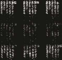 |
| Because of the interference of the phase-shifted light beams emitted by the antennas, images of the MIT logo appear to hover above the surface of the chip.
Image: Jie Sun |
Abstract:
f you want to create a moving light source, you have a few possibilities. One is to mount a light emitter in some kind of mechanical housing — the approach used in, say, theatrical spotlights, which stagehands swivel and tilt to track performers.
Chips that can steer light: Record-setting ‘optical phased arrays’ could lead to better laser rangefinders, smaller medical-imaging devices and even holographic TVs
Cambridge, MA | Posted on January 11th, 2013Another possibility, however, is to create an array of light emitters and vary their "phase" — the alignment of the light waves they produce. The out-of-phase light waves interfere with one another, reinforcing each other in some directions but annihilating each other in others. The result is a light source that doesn't move, but can project a beam in any direction.
Such "phased arrays" have been around for more than a century, used most commonly in radar transmitters, which can be as much as 100 feet tall. But in this week's issue of Nature, researchers from MIT's Research Laboratory of Electronics (RLE) describe a 4,096-emitter array that fits on a single silicon chip. Chips that can steer beams of light could enable a wide range of applications, including cheaper, more efficient, and smaller laser rangefinders; medical-imaging devices that can be threaded through tiny blood vessels; and even holographic televisions that emit different information when seen from different viewing angles.
In their Nature paper, the MIT authors — Michael Watts, an associate professor of electrical engineering, Jie Sun, a graduate student in Watts' lab and first author on the paper, Sun's fellow graduate students Erman Timurdogan and Ami Yaacobi, and Ehsan Shah Hosseini, an RLE postdoc — report on two new chips. Both chips take in laser light and re-emit it via tiny antennas etched into the chip surface.
Calculated incoherence
A wave of light can be thought of as a sequence of crests and troughs, just like those of an ocean wave. Laser light is coherent, meaning that the waves composing it are in phase: Their troughs and crests are perfectly aligned. The antennas in the RLE researchers' chips knock that coherent light slightly out of phase, producing interference patterns.
In the 4,096-antenna chip — a 64-by-64 grid of antennas — the phase shifts are precalculated to produce rows of images of the MIT logo. The antennas are not simply turned off and on in a pattern that traces the logo, as the pixels in a black-and-white monitor would be. All of the antennas emit light, and if you were close enough to them (and had infrared vision), you would see a regular array of pinpricks of light. Seen from more than a few millimeters away, however, the interference of the antennas' phase-shifted beams produces a more intricate image.
In the other chip, which has an eight-by-eight grid of antennas, the phase shift produced by the antennas is tunable, so the chip can steer light in arbitrary directions. In both chips, the design of the antenna is the same; in principle, the researchers could have built tuning elements into the antennas of the larger chip. But "there would be too many wires coming off the chip," Watts says. "Four thousand wires is more than Jie wanted to solder up."
Indeed, Watts explains, wiring limitations meant that even the smaller chip is tunable only a row or column at a time. But that's enough to produce some interesting interference patterns that demonstrate that the tuning elements are working. The large chip, too, largely constitutes a proof of principle, Watts says. "It's kind of amazing that this actually worked," he says. "It's really nanometer precision of the phase, and you're talking about a fairly large chip."
Precision engineering
In both chips, laser light is conducted across the chip by silicon ridges known as "waveguides." Drawing light from the optical signal attenuates it, so antennas close to the laser have to draw less light than those farther away. If the calculation of either the attenuation of the signal or the variation in the antennas' design is incorrect, the light emitted by the antennas could vary too much to be useful.
Both chips represent the state of the art in their respective classes. No two-dimensional tunable phased array has previously been built on a chip, and the largest previous non-tunable (or "passive") array had only 16 antennas. Nonetheless, "I think we can go to much, much larger arrays," Watts says. "It's now very believable that we could make a 3-D holographic display."
"I think it's one of the first clearly competitive applications where photonics wins," says Michal Lipson, an associate professor of electrical and computer engineering at Cornell University and head of the Cornell Nanophotonics Group. Within the photonics community, Lipson says, most work is geared toward "the promise that if photonics is embedded in electronic systems, it's going to really improve things. Here, [the MIT team] has developed a complete system. It's not a small component: This system is ready to go. So it's very convincing."
Lipson adds that the tuning limitations of the MIT researchers' prototype chips is no reason to doubt the practicality of the design. "It's just physically hard to come up with a very high number of contacts that are external," she says. "Now, if you were to integrate everything so that it's all on silicon, there shouldn't be any problem to integrate those contacts."
####
For more information, please click here
Contacts:
Sarah McDonnell
617-253-8923
Copyright © Massachusetts Institute of Technology
If you have a comment, please Contact us.Issuers of news releases, not 7th Wave, Inc. or Nanotechnology Now, are solely responsible for the accuracy of the content.
Bookmark:


| Related News Press |
News and information
![]() Simulating magnetization in a Heisenberg quantum spin chain April 5th, 2024
Simulating magnetization in a Heisenberg quantum spin chain April 5th, 2024
![]() NRL charters Navy’s quantum inertial navigation path to reduce drift April 5th, 2024
NRL charters Navy’s quantum inertial navigation path to reduce drift April 5th, 2024
![]() Discovery points path to flash-like memory for storing qubits: Rice find could hasten development of nonvolatile quantum memory April 5th, 2024
Discovery points path to flash-like memory for storing qubits: Rice find could hasten development of nonvolatile quantum memory April 5th, 2024
![]() Good as gold - improving infectious disease testing with gold nanoparticles April 5th, 2024
Good as gold - improving infectious disease testing with gold nanoparticles April 5th, 2024
Display technology/LEDs/SS Lighting/OLEDs
![]() Utilizing palladium for addressing contact issues of buried oxide thin film transistors April 5th, 2024
Utilizing palladium for addressing contact issues of buried oxide thin film transistors April 5th, 2024
![]() Light guide plate based on perovskite nanocomposites November 3rd, 2023
Light guide plate based on perovskite nanocomposites November 3rd, 2023
![]() Simple ballpoint pen can write custom LEDs August 11th, 2023
Simple ballpoint pen can write custom LEDs August 11th, 2023
Chip Technology
![]() Discovery points path to flash-like memory for storing qubits: Rice find could hasten development of nonvolatile quantum memory April 5th, 2024
Discovery points path to flash-like memory for storing qubits: Rice find could hasten development of nonvolatile quantum memory April 5th, 2024
![]() Utilizing palladium for addressing contact issues of buried oxide thin film transistors April 5th, 2024
Utilizing palladium for addressing contact issues of buried oxide thin film transistors April 5th, 2024
![]() HKUST researchers develop new integration technique for efficient coupling of III-V and silicon February 16th, 2024
HKUST researchers develop new integration technique for efficient coupling of III-V and silicon February 16th, 2024
Optical computing/Photonic computing
![]() With VECSELs towards the quantum internet Fraunhofer: IAF achieves record output power with VECSEL for quantum frequency converters April 5th, 2024
With VECSELs towards the quantum internet Fraunhofer: IAF achieves record output power with VECSEL for quantum frequency converters April 5th, 2024
![]() Chemical reactions can scramble quantum information as well as black holes April 5th, 2024
Chemical reactions can scramble quantum information as well as black holes April 5th, 2024
![]() Optically trapped quantum droplets of light can bind together to form macroscopic complexes March 8th, 2024
Optically trapped quantum droplets of light can bind together to form macroscopic complexes March 8th, 2024
![]() HKUST researchers develop new integration technique for efficient coupling of III-V and silicon February 16th, 2024
HKUST researchers develop new integration technique for efficient coupling of III-V and silicon February 16th, 2024
Discoveries
![]() Chemical reactions can scramble quantum information as well as black holes April 5th, 2024
Chemical reactions can scramble quantum information as well as black holes April 5th, 2024
![]() New micromaterial releases nanoparticles that selectively destroy cancer cells April 5th, 2024
New micromaterial releases nanoparticles that selectively destroy cancer cells April 5th, 2024
![]() Utilizing palladium for addressing contact issues of buried oxide thin film transistors April 5th, 2024
Utilizing palladium for addressing contact issues of buried oxide thin film transistors April 5th, 2024
Announcements
![]() NRL charters Navy’s quantum inertial navigation path to reduce drift April 5th, 2024
NRL charters Navy’s quantum inertial navigation path to reduce drift April 5th, 2024
![]() Discovery points path to flash-like memory for storing qubits: Rice find could hasten development of nonvolatile quantum memory April 5th, 2024
Discovery points path to flash-like memory for storing qubits: Rice find could hasten development of nonvolatile quantum memory April 5th, 2024
Photonics/Optics/Lasers
![]() With VECSELs towards the quantum internet Fraunhofer: IAF achieves record output power with VECSEL for quantum frequency converters April 5th, 2024
With VECSELs towards the quantum internet Fraunhofer: IAF achieves record output power with VECSEL for quantum frequency converters April 5th, 2024
![]() Nanoscale CL thermometry with lanthanide-doped heavy-metal oxide in TEM March 8th, 2024
Nanoscale CL thermometry with lanthanide-doped heavy-metal oxide in TEM March 8th, 2024
![]() Optically trapped quantum droplets of light can bind together to form macroscopic complexes March 8th, 2024
Optically trapped quantum droplets of light can bind together to form macroscopic complexes March 8th, 2024
![]() HKUST researchers develop new integration technique for efficient coupling of III-V and silicon February 16th, 2024
HKUST researchers develop new integration technique for efficient coupling of III-V and silicon February 16th, 2024
|
|
||
|
|
||
| The latest news from around the world, FREE | ||
|
|
||
|
|
||
| Premium Products | ||
|
|
||
|
Only the news you want to read!
Learn More |
||
|
|
||
|
Full-service, expert consulting
Learn More |
||
|
|
||