Home > Press > Long-wavelength laser will be able to take medicine fingerprints
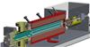 |
| Cross-section of a prototype pFEL, with the free electron source on the right and the photonic crystal inside the red part. |
Abstract:
A laser capable of working in the terahertz range - that of long-wavelength light from the far infrared to 1 millimetre - enables the ‘fingerprint' of, say, a drug to be examined better than can be done using chemical analysis. To achieve this, PhD student Thomas Denis of the University of Twente's MESA+ Institute for Nanotechnology has combined the best of two worlds, a free electron source and photonic crystals. The result: greater flexibility and a compact laser.
Long-wavelength laser will be able to take medicine fingerprints
Enschede, Netherlands | Posted on December 20th, 2012A terahertz laser is capable of showing the molecular structure of, say, a drug, because the laser beam it produces is at wavelengths suitable for examining molecular and atomic bonds. This enables more spatial information to be obtained than from chemical analysis, a detailed fingerprint. To date, however, the limitation has been that lasers of this type are restricted to particular wavelengths, e.g. because the source of the laser light is a semiconductor, in which electrons can only take on fixed energy states, hence only a limited number of ‘colours' of light can be produced.
Free electrons
In a free electron laser the electrons are not restricted to fixed states, as are electrons in a classic cathode ray tube. So Denis thought, why not combine a free electron source with a ‘photonic crystal'? This is a structure with lot of tiny ‘posts' that together slow down the incident light and turn it into a coherent beam. Photonic crystals can be created at micro level, e.g. for a lab-on-a-chip, or on a much larger scale. The dimensions and shape of the crystal determine the rough wavelength region, and the precise wavelength can be set and adjusted by changing the speed of the electrons being fired at it. This combination is known as a ‘photonic free-electron laser' or pFEL.
Looking inside the crystal
Existing terahertz lasers also have the disadvantage that they are very large, big enough to fill a room. Thanks to the use of photonic crystals the pFEL that Denis has designed is not much bigger than a domestic microwave oven and can still provide high power despite its small size. He has also found a special way of ‘looking' inside a photonic crystal - something that is not normally possible. By interfering slightly with the wavelength pattern in the crystal using a tiny metal ball the actual pattern can be measured.
Thomas Denis (Ahaus, 1981) received his PhD on 14 December for his thesis Theory and Design of Microwave Photonic Free-Electron Lasers. He carried out his research in Prof. Klaus Boller's Laser Physics and Non-linear Optics Group. The thesis, or the summary, is available in digital form on request.
####
For more information, please click here
Contacts:
P.O. Box 217
7500 AE Enschede, Netherlands
053-489 9111
053-489 2000
Wiebe van der Veen
+31612185692
Copyright © AlphaGalileo
If you have a comment, please Contact us.Issuers of news releases, not 7th Wave, Inc. or Nanotechnology Now, are solely responsible for the accuracy of the content.
Bookmark:


| Related News Press |
News and information
![]() Simulating magnetization in a Heisenberg quantum spin chain April 5th, 2024
Simulating magnetization in a Heisenberg quantum spin chain April 5th, 2024
![]() NRL charters Navy’s quantum inertial navigation path to reduce drift April 5th, 2024
NRL charters Navy’s quantum inertial navigation path to reduce drift April 5th, 2024
![]() Discovery points path to flash-like memory for storing qubits: Rice find could hasten development of nonvolatile quantum memory April 5th, 2024
Discovery points path to flash-like memory for storing qubits: Rice find could hasten development of nonvolatile quantum memory April 5th, 2024
Nanomedicine
![]() New micromaterial releases nanoparticles that selectively destroy cancer cells April 5th, 2024
New micromaterial releases nanoparticles that selectively destroy cancer cells April 5th, 2024
![]() Good as gold - improving infectious disease testing with gold nanoparticles April 5th, 2024
Good as gold - improving infectious disease testing with gold nanoparticles April 5th, 2024
![]() Researchers develop artificial building blocks of life March 8th, 2024
Researchers develop artificial building blocks of life March 8th, 2024
Discoveries
![]() Chemical reactions can scramble quantum information as well as black holes April 5th, 2024
Chemical reactions can scramble quantum information as well as black holes April 5th, 2024
![]() New micromaterial releases nanoparticles that selectively destroy cancer cells April 5th, 2024
New micromaterial releases nanoparticles that selectively destroy cancer cells April 5th, 2024
![]() Utilizing palladium for addressing contact issues of buried oxide thin film transistors April 5th, 2024
Utilizing palladium for addressing contact issues of buried oxide thin film transistors April 5th, 2024
Announcements
![]() NRL charters Navy’s quantum inertial navigation path to reduce drift April 5th, 2024
NRL charters Navy’s quantum inertial navigation path to reduce drift April 5th, 2024
![]() Discovery points path to flash-like memory for storing qubits: Rice find could hasten development of nonvolatile quantum memory April 5th, 2024
Discovery points path to flash-like memory for storing qubits: Rice find could hasten development of nonvolatile quantum memory April 5th, 2024
Tools
![]() Ferroelectrically modulate the Fermi level of graphene oxide to enhance SERS response November 3rd, 2023
Ferroelectrically modulate the Fermi level of graphene oxide to enhance SERS response November 3rd, 2023
![]() The USTC realizes In situ electron paramagnetic resonance spectroscopy using single nanodiamond sensors November 3rd, 2023
The USTC realizes In situ electron paramagnetic resonance spectroscopy using single nanodiamond sensors November 3rd, 2023
Photonics/Optics/Lasers
![]() With VECSELs towards the quantum internet Fraunhofer: IAF achieves record output power with VECSEL for quantum frequency converters April 5th, 2024
With VECSELs towards the quantum internet Fraunhofer: IAF achieves record output power with VECSEL for quantum frequency converters April 5th, 2024
![]() Nanoscale CL thermometry with lanthanide-doped heavy-metal oxide in TEM March 8th, 2024
Nanoscale CL thermometry with lanthanide-doped heavy-metal oxide in TEM March 8th, 2024
![]() Optically trapped quantum droplets of light can bind together to form macroscopic complexes March 8th, 2024
Optically trapped quantum droplets of light can bind together to form macroscopic complexes March 8th, 2024
![]() HKUST researchers develop new integration technique for efficient coupling of III-V and silicon February 16th, 2024
HKUST researchers develop new integration technique for efficient coupling of III-V and silicon February 16th, 2024
|
|
||
|
|
||
| The latest news from around the world, FREE | ||
|
|
||
|
|
||
| Premium Products | ||
|
|
||
|
Only the news you want to read!
Learn More |
||
|
|
||
|
Full-service, expert consulting
Learn More |
||
|
|
||