Home > Press > Engineers roll up their sleeves ' and then do the same with inductors
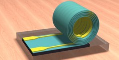 |
| Illinois researchers developed a new design paradigm for inductors. Processed while flat, they then roll up on their own, taking up much less space on a chip. |
Abstract:
On the road to smaller, high-performance electronics, University of Illinois researchers have smoothed one speed bump by shrinking a key, yet notoriously large element of integrated circuits.
Engineers roll up their sleeves ' and then do the same with inductors
Champaign, IL | Posted on December 13th, 2012Three-dimensional rolled-up inductors have a footprint more than 100 times smaller without sacrificing performance. The researchers published their new design paradigm in the journal Nano Letters.
"It's a new concept for old technology," said team leader Xiuling Li, a professor of electrical and computer engineering at the University of Illinois.
Inductors, often seen as the sprawling metal spirals on computer chips, are essential components of integrated circuits. They store magnetic energy, acting as a buffer against changes in current and modulating frequency - especially important in radio-frequency wireless devices. However, they take up a lot of space. Inductance depends on the number of coils in the spiral, so engineers cannot make them smaller without losing performance.
In addition, the larger the area the inductor occupies, the more it interfaces with the substrate the chip is built on, exacerbating a hindering effect called parasitic capacitance. Researchers have developed some three-dimensional inductor structures to solve the dual problems of space and parasitic capacitance, but these methods are complex and use techniques that are difficult to scale up to manufacturing levels.
The new inductor design uses techniques Li's group previously developed for making thin films of silicon nitride, merely tens of nanometers in thickness, that roll themselves up into tubes. The research team used industry-standard two-dimensional processing to pattern metal lines on the film before rolling, creating a spiral inductor.
"We're making 3-D structures with 2-D processing," Li said. "Instead of spreading this out in a large area to increase inductance, we can have the same inductance but packed into a much smaller area."
Using the self-rolling technique, the researchers can shrink the area needed for a radio-frequency inductor to a scant 45 microns by 16 microns - more than 100 times smaller than the area an equivalent flat spiral would require.
The design can be adjusted to fit target parameters including metal thickness and type, frequency, tube diameter and number of turns. According to Li, this technique could be used for capacitors and other integrated circuit elements as well.
Now, Li's group is working to produce high-performance inductor prototypes, in collaboration with electrical and engineering professor Jose Schutt-Aine. Preliminary experimental data show strong correlation with the modeled designs.
"Once we have optimized this process, we should be able to make an integrated circuit with a completely different platform that could be much smaller," Li said. "It's an ambitious goal."
The National Science Foundation and the Office of Naval Research supported this work. U. of I. visiting researcher Wen Huang, postdoctoral researcher Xin Yu, graduate student Paul Froeter and mechanical science and engineering professor Placid Ferreira were co-authors of this study. Li also is affiliated with the Beckman Institute for Advanced Science and Technology, the Micro and Nanotechnology Lab, and the Frederick Seitz Materials Research Lab, all at the U. of I.
####
For more information, please click here
Contacts:
Liz Ahlberg
Physical Sciences Editor
217-244-1073
Xiuling Li
217-265-6354
Copyright © University of Illinois at Urbana-Champaign
If you have a comment, please Contact us.Issuers of news releases, not 7th Wave, Inc. or Nanotechnology Now, are solely responsible for the accuracy of the content.
Bookmark:


| Related Links |
| Related News Press |
News and information
![]() Simulating magnetization in a Heisenberg quantum spin chain April 5th, 2024
Simulating magnetization in a Heisenberg quantum spin chain April 5th, 2024
![]() NRL charters Navy�s quantum inertial navigation path to reduce drift April 5th, 2024
NRL charters Navy�s quantum inertial navigation path to reduce drift April 5th, 2024
![]() Discovery points path to flash-like memory for storing qubits: Rice find could hasten development of nonvolatile quantum memory April 5th, 2024
Discovery points path to flash-like memory for storing qubits: Rice find could hasten development of nonvolatile quantum memory April 5th, 2024
Hardware
![]() The present and future of computing get a boost from new research July 21st, 2023
The present and future of computing get a boost from new research July 21st, 2023
![]() A Carbon Nanotube Microprocessor Mature Enough to Say Hello: Three new breakthroughs make commercial nanotube processors possible March 2nd, 2020
A Carbon Nanotube Microprocessor Mature Enough to Say Hello: Three new breakthroughs make commercial nanotube processors possible March 2nd, 2020
![]() Powering the future: Smallest all-digital circuit opens doors to 5 nm next-gen semiconductor February 11th, 2020
Powering the future: Smallest all-digital circuit opens doors to 5 nm next-gen semiconductor February 11th, 2020
Govt.-Legislation/Regulation/Funding/Policy
![]() NRL charters Navy�s quantum inertial navigation path to reduce drift April 5th, 2024
NRL charters Navy�s quantum inertial navigation path to reduce drift April 5th, 2024
![]() Discovery points path to flash-like memory for storing qubits: Rice find could hasten development of nonvolatile quantum memory April 5th, 2024
Discovery points path to flash-like memory for storing qubits: Rice find could hasten development of nonvolatile quantum memory April 5th, 2024
![]() Chemical reactions can scramble quantum information as well as black holes April 5th, 2024
Chemical reactions can scramble quantum information as well as black holes April 5th, 2024
Chip Technology
![]() Discovery points path to flash-like memory for storing qubits: Rice find could hasten development of nonvolatile quantum memory April 5th, 2024
Discovery points path to flash-like memory for storing qubits: Rice find could hasten development of nonvolatile quantum memory April 5th, 2024
![]() Utilizing palladium for addressing contact issues of buried oxide thin film transistors April 5th, 2024
Utilizing palladium for addressing contact issues of buried oxide thin film transistors April 5th, 2024
![]() HKUST researchers develop new integration technique for efficient coupling of III-V and silicon February 16th, 2024
HKUST researchers develop new integration technique for efficient coupling of III-V and silicon February 16th, 2024
Discoveries
![]() Chemical reactions can scramble quantum information as well as black holes April 5th, 2024
Chemical reactions can scramble quantum information as well as black holes April 5th, 2024
![]() New micromaterial releases nanoparticles that selectively destroy cancer cells April 5th, 2024
New micromaterial releases nanoparticles that selectively destroy cancer cells April 5th, 2024
![]() Utilizing palladium for addressing contact issues of buried oxide thin film transistors April 5th, 2024
Utilizing palladium for addressing contact issues of buried oxide thin film transistors April 5th, 2024
Announcements
![]() NRL charters Navy�s quantum inertial navigation path to reduce drift April 5th, 2024
NRL charters Navy�s quantum inertial navigation path to reduce drift April 5th, 2024
![]() Discovery points path to flash-like memory for storing qubits: Rice find could hasten development of nonvolatile quantum memory April 5th, 2024
Discovery points path to flash-like memory for storing qubits: Rice find could hasten development of nonvolatile quantum memory April 5th, 2024
Interviews/Book Reviews/Essays/Reports/Podcasts/Journals/White papers/Posters
![]() Simulating magnetization in a Heisenberg quantum spin chain April 5th, 2024
Simulating magnetization in a Heisenberg quantum spin chain April 5th, 2024
![]() Discovery points path to flash-like memory for storing qubits: Rice find could hasten development of nonvolatile quantum memory April 5th, 2024
Discovery points path to flash-like memory for storing qubits: Rice find could hasten development of nonvolatile quantum memory April 5th, 2024
Military
![]() NRL charters Navy�s quantum inertial navigation path to reduce drift April 5th, 2024
NRL charters Navy�s quantum inertial navigation path to reduce drift April 5th, 2024
![]() What heat can tell us about battery chemistry: using the Peltier effect to study lithium-ion cells March 8th, 2024
What heat can tell us about battery chemistry: using the Peltier effect to study lithium-ion cells March 8th, 2024
![]() New chip opens door to AI computing at light speed February 16th, 2024
New chip opens door to AI computing at light speed February 16th, 2024
|
|
||
|
|
||
| The latest news from around the world, FREE | ||
|
|
||
|
|
||
| Premium Products | ||
|
|
||
|
Only the news you want to read!
Learn More |
||
|
|
||
|
Full-service, expert consulting
Learn More |
||
|
|
||